Altera Arria V SoC User Manual
Page 14
3–4
Chapter 3: Board Setup and Defaults
Factory Default Switch and Jumper Settings
Arria V SoC Development Kit
June 2014
Altera Corporation
User Guide
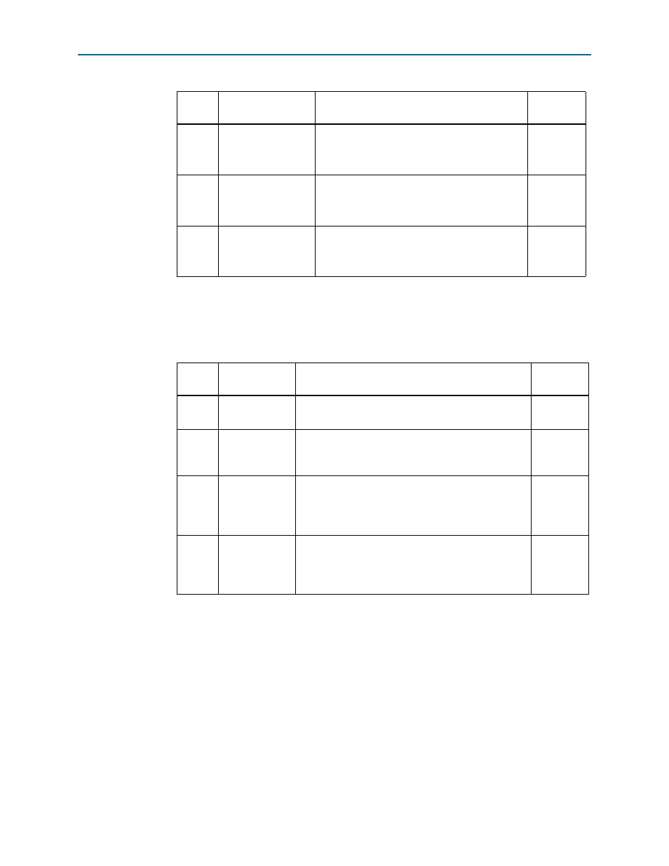
3. Set the DIP switch bank (SW4) to match
and
.
In the following table, up and down indicates the position of the switch with the
board orientation as shown in
3
MSEL2
Switch 3 has the following options:
■
ON (up) = MSEL2 is 0.
■
OFF (down) = MSEL2 is 1.
ON
4
MSEL3
Switch 4 has the following options:
■
ON (up) = MSEL3 is 0.
■
OFF (down) = MSEL3 is 1.
ON
5
MSEL4
Switch 5 has the following options:
■
ON (up) = MSEL4 is 0.
■
OFF (down) = MSEL4 is 1.
ON
Table 3–3. SW4 JTAG DIP Switch Settings
Switch
Board
Label
Function
Default
Position
1
HPS
■
ON (up) = Do not Include HPS in the JTAG chain.
■
OFF (down) = Include HPS in the JTAG chain
OFF
2
FPGA
■
ON (up) = Do not Include the FPGA in the JTAG
chain.
■
OFF (down) = Include the FPGA in the JTAG chain.
OFF
3
FMCA
■
ON (up) = Do not include the FMCA connector in the
JTAG chain.
■
OFF (down) = Include the FMCA connector in the
JTAG chain.
ON
4
MAX
■
ON (up) = Do not include the MAX V system
controller in the JTAG chain.
■
OFF (down) = Include the MAX V system controller in
the JTAG chain.
OFF
Table 3–2. SW3 DIP Switch Settings (Part 2 of 2)
Switch
Board
Label
Function
Default
Position