Using the board test system, The configure menu, The system info tab – Altera Arria V SoC User Manual
Page 23: Using the board test system –3, The configure menu –3 the system info tab –3
Chapter 5: Board Test System
5–3
Using the Board Test System
June 2014
Altera Corporation
Arria V SoC Development Kit
User Guide
A GUI appears, displaying the application tab that corresponds to the design running
in the FPGA. The Arria V development board’s flash memory ships preconfigured
with the design that corresponds to the GPIO tab.
1
Under two conditions, the BTS displays a message prompting you to configure your
board with a valid BTS design:
■
If you power up your board with the DIP switch (SW2.3) in a position other than
the on (0) position
■
If you load your own design into the FPGA with the Quartus II Programmer
Using the Board Test System
This section describes each control in the BTS.
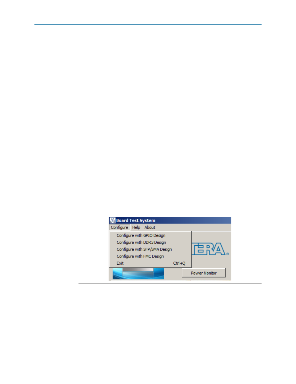
The Configure Menu
Use the Configure menu to select the design you want to use. Each design example on
this menu tests different board features that corresponds to one or more application
tabs. For example, if you select Configure with GPIO Design, the System Info,
GPIO
, and I2C tabs become available for testing.
c
The BTS configuration circuit might cause a conflict with the default HPS booting
sequence. Both events program the FPGA. To make sure the operation of the
Configure menu works properly, wait until you see the LCD display Hello Tim before
you use the Configure menu.
The System Info Tab
The System Info tab shows board’s current configuration.
shows the System Info tab. The tab displays the contents of the MAX V registers, the
JTAG chain, the board’s MAC address, the flash memory map, and other details
stored on the board.
The following sections describe the controls on the System Info tab.
Figure 5–2. The Configure Menu