Altera Arria II GX FPGA Development Board, 6G Edition User Manual
Page 18
2–10
Chapter 2: Board Components
MAX II CPLD EPM2210 System Controller
Arria II GX FPGA Development Board, 6G Edition Reference Manual
© July 2010 Altera Corporation
fsm_d[21]
2.5-V
D1
T10
FSM bus data
fsm_d[22]
2.5-V
F1
P4
FSM bus data
fsm_d[23]
2.5-V
F3
R11
FSM bus data
fsm_d[24]
2.5-V
G2
A18
FSM bus data
fsm_d[25]
2.5-V
F2
B18
FSM bus data
fsm_d[26]
2.5-V
G3
C19
FSM bus data
fsm_d[27]
2.5-V
G1
D19
FSM bus data
fsm_d[28]
2.5-V
H1
B21
FSM bus data
fsm_d[29]
2.5-V
G4
A21
FSM bus data
fsm_d[3]
2.5-V
C14
B19
FSM bus data
fsm_d[30]
2.5-V
J4
C21
FSM bus data
fsm_d[31]
2.5-V
H2
A22
FSM bus data
fsm_d[4]
2.5-V
E8
E19
FSM bus data
fsm_d[5]
2.5-V
D4
E18
FSM bus data
fsm_d[6]
2.5-V
C6
G19
FSM bus data
fsm_d[7]
2.5-V
D5
F19
FSM bus data
fsm_d[8]
2.5-V
E6
D21
FSM bus data
fsm_d[9]
2.5-V
D14
D23
FSM bus data
hsma_psnt_n
2.5-V
A10
U3
HSMC port A present
hsmb_psnt_n
2.5-V
J13
AG28
HSMC port B present
led_config_led[0]
2.5-V
B8
—
Flash memory image select indicator
led_config_led[1]
2.5-V
A8
—
Flash memory image select indicator
led_config_led[2]
2.5-V
B7
—
Flash memory image select indicator
factory
(IMAGE SEL)
2.5-V
B9
—
Toggles the LED_CONFIG_LED[2:0]
sequence.
lcd_pwrmon
2.5-V
K13
—
DIP - MAX II LCD drive enable
reset_confign
(LOAD IMAGE)
2.5-V
A9
—
Load the flash memory identified by the
configuration LEDs
max_dip[0]
2.5-V
L16
—
DIP - reserved
max_dip[1]
2.5-V
L15
—
DIP - reserved
max_dip[2]
2.5-V
L14
—
DIP - reserved
max_error
2.5-V
B10
—
FPGA configuration error LED
max_led
2.5-V
B11
—
LED - reserved
max_load
2.5-V
A11
—
FPGA configuration active LED
max_resetn
2.5-V
M9
—
MAX II reset push-button
max2_ben[0]
2.5-V
M11
C15
FSM bus Max2 byte enable 0
max2_ben[1]
2.5-V
M10
H16
FSM bus Max2 byte enable 1
max2_ben[2]
2.5-V
N12
D14
FSM bus Max2 byte enable 2
max2_ben[3]
2.5-V
P12
A9
FSM bus Max2 byte enable 3
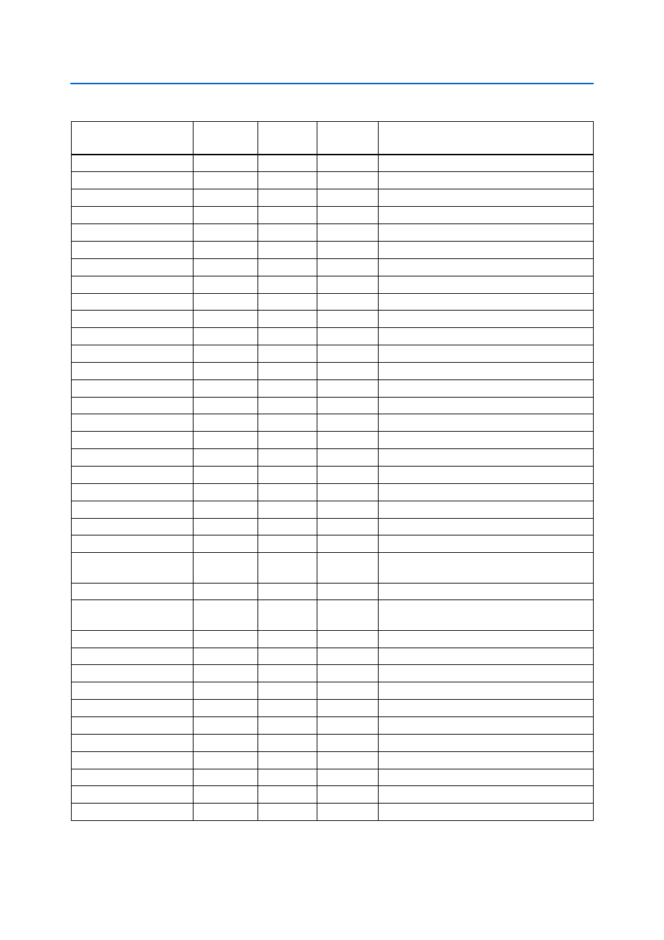
Table 2–6. MAX II CPLD EPM2210 System Controller Device Pin-Out (Part 4 of 5)
Schematic Signal Name
I/O Standard
EPM2210
Pin Number
EP2AGX125
Pin Number
Description