Altera Arria II GX FPGA Development Board, 6G Edition User Manual
Page 29
Chapter 2: Board Components
2–21
Clock Circuitry
© July 2010 Altera Corporation
Arria II GX FPGA Development Board, 6G Edition Reference Manual
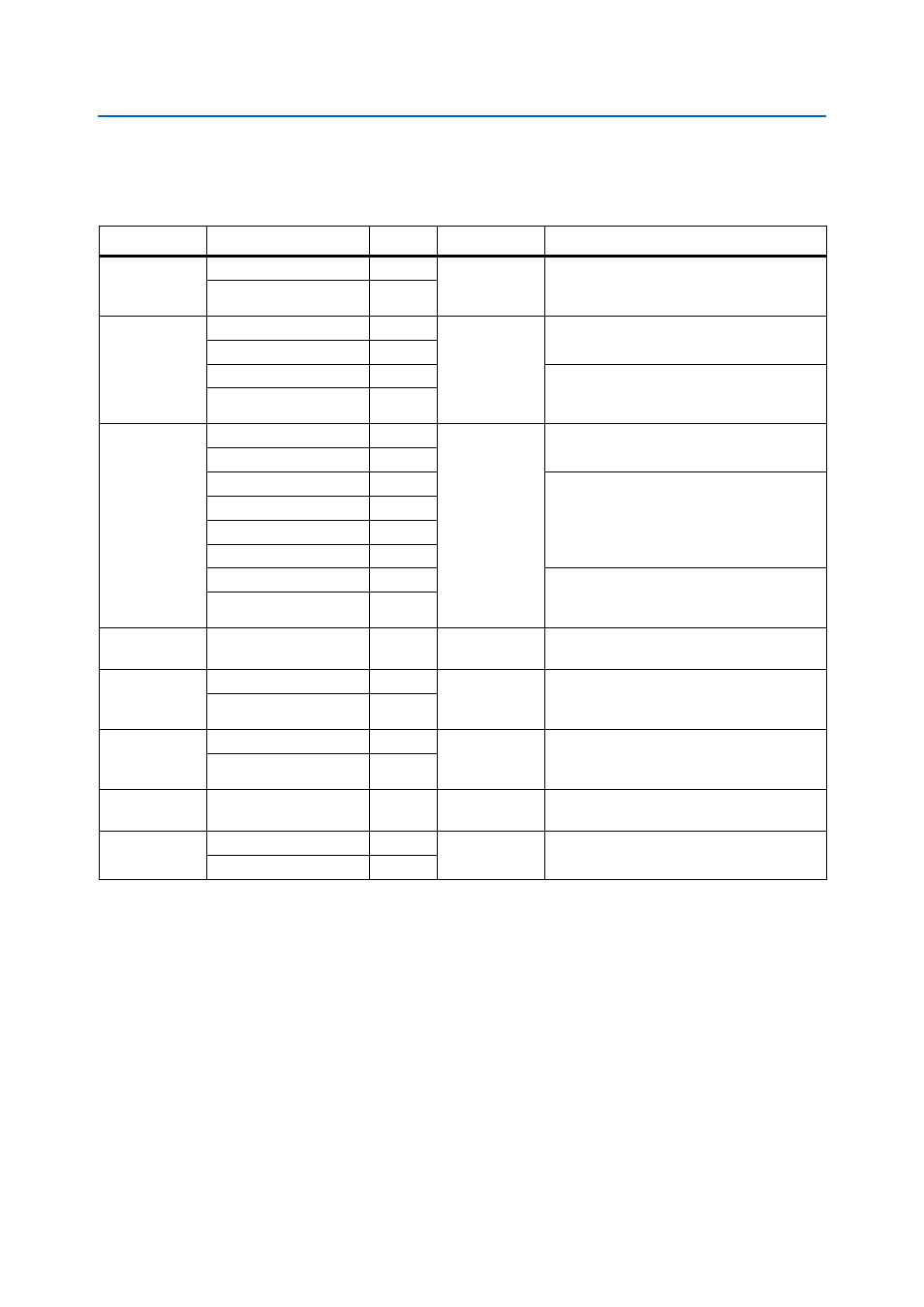
shows the external clock inputs for the Arria II GX FPGA development
board, 6G Edition.
Table 2–19. Arria II GX FPGA Development Board, 6G Edition Clock Inputs
Source
Schematic Signal Name
Pin
I/O Standard
Description
U25
CLK_155_P
R29
LVPECL
155.52 MHz oscillator which drives the
transceiver Q2 reference clock input with
100
Ω OCT.
CLK_155_N
R30
SMA or
100.000 MHz
(Default
Frequency)
CLKIN_BOT_P
AJ19
LVDS
Input to the fan-out buffer (U33) which drives
LVDS input to the bottom edge of PLL input.
CLKIN_BOT_N
AK19
CLKIN_REF_Q2_P
U29
Input to the fan-out buffer (U33) which drives
LVDS input to the transceiver Q2 reference
clock input with 100
Ω OCT.
CLKIN_REF_Q2_N
U30
125.000 MHz
(Default
Frequency)
CLKIN_TOP_P
F18
LVDS
Programmable oscillator which drives LVDS
input to the top edge of PLL input.
CLKIN_TOP_N
F17
CLK_REF_Q1_1_P
AA29
Programmable oscillator which drives LVDS
input to the transceiver Q1 reference clock
input with 100
Ω OCT.
CLK_REF_Q1_1_N
AA30
CLK_REF_Q1_2_P
W29
CLK_REF_Q1_2_N
W30
CLK_REF_Q3_P
N29
Programmable oscillator which drives LVDS
input to the transceiver Q3 reference clock
input with 100
Ω OCT.
CLK_REF_Q3_N
N30
Samtec HSMC
HSMA_CLKIN0
AP17
LVTTL
Single-ended input from the installed HSMC
port A cable or board.
Samtec HSMC
HSMA_CLKIN_P1
U6
LVDS or LVTTL
LVDS input from the installed HSMC port A
cable or board. Can also support two LVTTL
inputs.
HSMA_CLKIN_N1
U5
Samtec HSMC
HSMA_CLKIN_P2
K18
LVDS or LVTTL
LVDS input from the installed HSMC port A
cable or board. Can also support two LVTTL
inputs.
HSMA_CLKIN_N2
J18
Samtec HSMC
HSMB_CLKIN0
AP16
LVTTL
Single-ended input from the installed HSMC
port B cable or board.
PCI Express
Edge
PCIE_REFCLK_P
AE29
HCSL
High-Speed Current Steering Logic (HCSL)
input from the PCI Express edge connector.
PCIE_REFCLK_N
AE30
Notes to
:
(1) CDCM61001 has a default frequency of 100 MHz, but can also be set by the MAX II CPLD to frequencies of 125 MHz and 156.25 MHz.
(2) CDCM61004 has a default frequency of 125 MHz, but can also be set by the MAX II CPLD to frequencies of 100 MHz and 156.25 MHz.