Altera Arria II GX FPGA Development Board, 6G Edition User Manual
Page 36
2–28
Chapter 2: Board Components
Components and Interfaces
Arria II GX FPGA Development Board, 6G Edition Reference Manual
© July 2010 Altera Corporation
The PCIE_REFCLK_P signal is a 100 MHz differential input that is driven from the PC
motherboard on to this board through the edge connector. This signal is connected
directly to a Arria II GX REFCLK input pin pair using DC coupling. This clock is
terminated on the motherboard and therefore, no on-board termination is required.
This clock can have spread-spectrum properties that change its period between
9.847 ps to 10.203 ps. The I/O standard is HCSL.
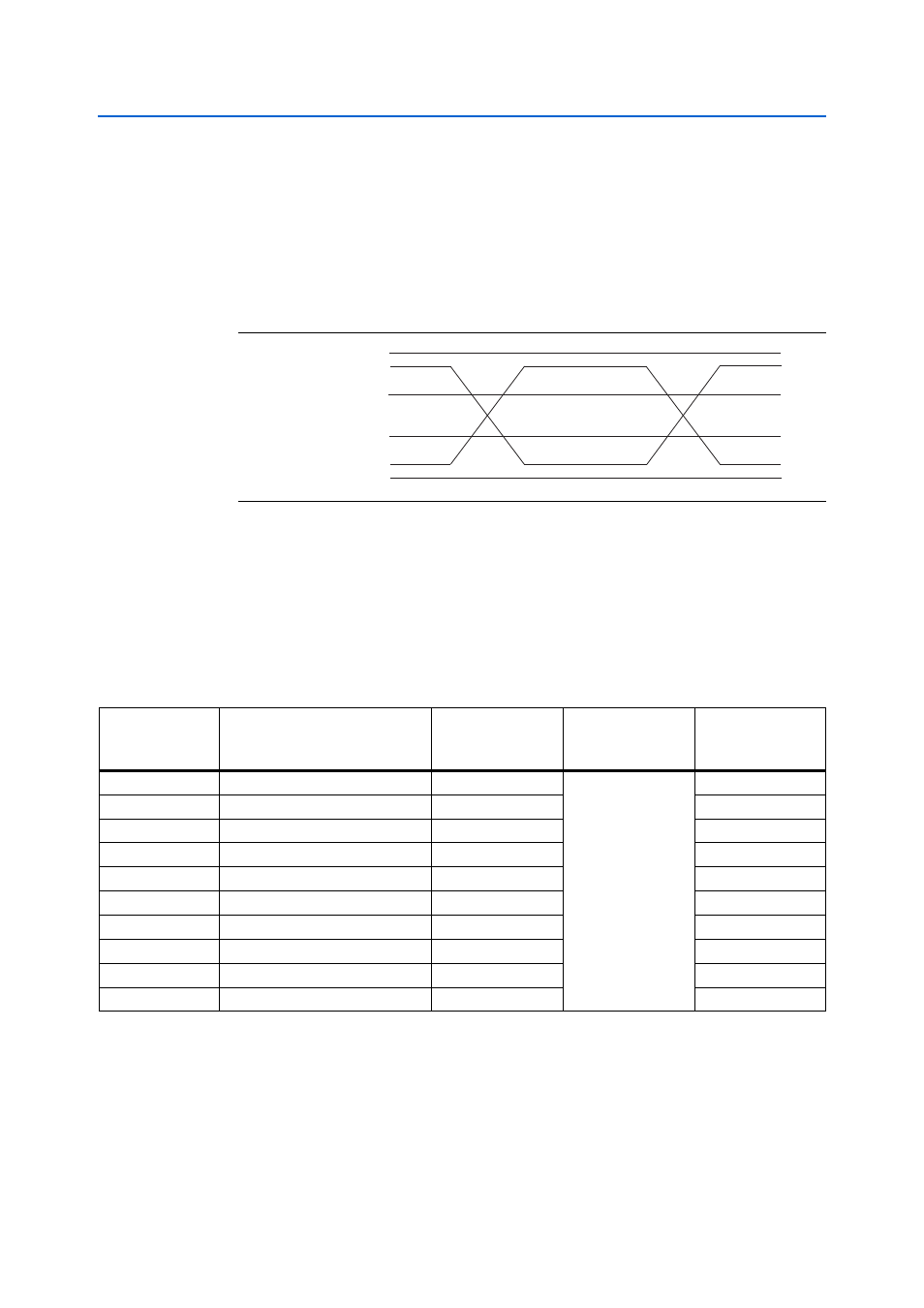
shows the PCI Express reference clock levels.
The JTAG and SMB are optional signals in the PCI Express specification. Both types of
signals are wired to the Arria II GX device but are not required for normal operation.
The PCI Express control DIP switch allows the presence detect grounding to be
altered to enable a ×1, ×4, or ×8 width edge connector. The PCI Express control DIP
switch does not support auto-negotiation.
summarizes the PCI Express pin assignments. The signal names and
directions are relative to the Arria II GX FPGA.
Figure 2–8. PCI Express Reference Clock Levels
V
MAX
= 1.15 V
V
CROSS MAX
= 550 mV
V
CROSS MIN
= 250 mV
V
MIN
= –0.30 V
REFCLK –
REFCLK +
Table 2–33. PCI Express Pin Assignments, Schematic Signal Names, and Functions (Part 1 of 2)
Board Reference
Description
Schematic Signal
Name
I/O Standard
Arria II GX Device
Pin Number
J14.B14
Add-in card receive bus
PCIE_RX_P0
1.5-V PCML
AN33
J14.B15
Add-in card receive bus
PCIE_RX_N0
AN34
J14.B19
Add-in card receive bus
PCIE_RX_P1
AL33
J14.B20
Add-in card receive bus
PCIE_RX_N1
AL34
J14.B23
Add-in card receive bus
PCIE_RX_P2
AJ33
J14.B24
Add-in card receive bus
PCIE_RX_N2
AJ34
J14.B27
Add-in card receive bus
PCIE_RX_P3
AG33
J14.B28
Add-in card receive bus
PCIE_RX_N3
AG34
J14.B33
Add-in card receive bus
PCIE_RX_P4
AE33
J14.B34
Add-in card receive bus
PCIE_RX_N4
AE34