Adc clock tree – Altera Multiaxis Motor Control Board User Manual
Page 10
Page 10
Functional Description
Multiaxis Motor Control Board
February 2014
Altera Corporation
The following equation calculates the current in the third, V, phase:
I
v
= –I
u
–I
w
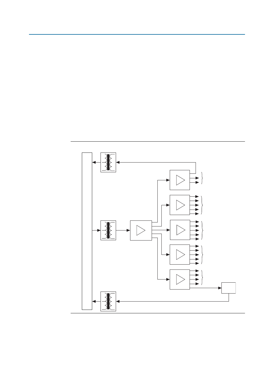
ADC Clock Tree
The 20-MHz ADC sample clock from the HSMC connector, CLK_HSMC_ADC, is buffered
by a tree of CDCLVC1106 low-skew clock buffers (
Figure 6
).
To compensate for the isolator device propagation delays, the HSMC connector
provides a feedback clock, CLK_HSMC_FEEDBACK, to the FPGA. The Multiaxis Motor
Control Board compensates for the isolator propagation delays, but you must still
account for the part-to-part skew when creating I/O timing constraints for the FPGA
design.
Alternatively, you can use a PLL in the FPGA to create a phase shifted version of the
ADC clock for sampling the inputs.
Figure 6. Clock Tree
TI CDCLVC116
1:6 Buffers
Motor
Channel 0
ADCs
Total Current
& DC Link
ADCs
ADC
ADC Data
Feedback Clock
Isolator
HSMC
Connector
Motor
Channel 1
ADCs
Motor
Channel 2
ADCs
Motor
Channel 3
ADCs