Factory- programmed reference design, Factory-programmed reference design –2 – Altera Nios Development Board Cyclone II Edition User Manual
Page 10
1–2
Reference Manual
Altera Corporation
Nios Development Board Cyclone II Edition
May 2007
Overview
f
See the Nios II Development Kit, Getting Started User Guide for instructions
on setting up the Nios development board and installing Nios II
development tools.
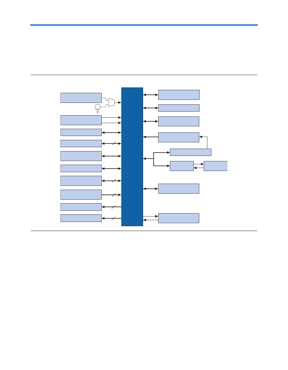
shows a block diagram of the Nios development board.
Figure 1–1. Nios Development Board, Cyclone II Edition Block Diagram
Factory-
Programmed
Reference
Design
When power is applied to the board, on-board logic configures the FPGA
using hardware configuration data stored in flash memory. After
successful configuration, the Nios II processor design in the FPGA wakes
up and begins executing boot code from flash memory.
The board is factory-programmed with a default reference design. This
reference design is a web server that delivers web pages via the Ethernet
port. For further information on the default reference design, refer to
Appendix B: Connecting to the Board via Ethernet.
Proto 2 Expansion
Prototype Connector
User LEDs (8)
Mictor Connector
Cyclone II
EP2C35
FPGA
41
4
8
Dual Seven-Segment Display
16
27
JTAG Connector
Proto 1 Expansion
Prototype Connector
Compact Flash
Push-button
Switches (4)
5.0 V Regulators
Vccint 1.2-V
Vccio 3.3-V
50MHz Oscillator
RS-232
PMC Connector
16 Mbyte DDR SDRAM
2 Mbyte SSRAM
Configuration
Controller
EPCS64 Configuration
Device
Ethernet
MAC/PHY
RJ45
Connector
16 Mbyte Flash Memory