Altera Nios Development Board Cyclone II Edition User Manual
Page 29
Altera Corporation
Reference Manual
2–17
May 2007
Nios Development Board Cyclone II Edition
Board Components
■
A buffered, zero-skew copy of the on-board oscillator output from
U2.
■
A buffered, zero-skew copy of the FPGA phase-locked loop (PLL)
output.
■
A logic-negative power-on reset signal.
■
Five regulated 3.3V power-supply pins (2A total max load for both
PROTO1 & PROTO2).
■
One regulated 5V power-supply pin (1A total max load for both
PROTO1 & PROTO2).
■
Numerous ground connections.
The PROTO1 expansion prototype connector shares FPGA I/O pins with
the CompactFlash connector (CON3). Designs can use either the PROTO1
connector or the CompactFlash connector.
1
Do not connect cards to PROTO1 and CON3 at the same time.
Damage to one or both cards might result.
f
See the Altera web site for a list of available expansion daughter cards
that can be used with the Nios development board at
www.altera.com/devkits.
show connections from the
PROTO1 expansion headers to the FPGA. Unless otherwise noted, labels
indicate FPGA pin numbers...
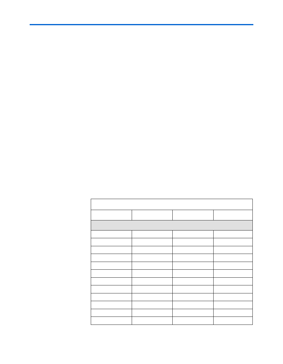
Table 2–11. PROTO1 Pin Table
FPGA Pin
PROTO1 Pin
Connector
Board Net Name
J11
U3 pin 56
1
J11
proto1_RESET_n
E25
3
J11
proto1_io0
F24
4
J11
proto1_io1
F23
5
J11
proto1_io2
J21
6
J11
proto1_io3
J20
7
J11
proto1_io4
F25
8
J11
proto1_io5
F26
9
J11
proto1_io6
N18
10
J11
proto1_io7
P18
11
J11
proto1_io8
G23
12
J11
proto1_io9
G24
13
J11
proto1_io10