Push-button switches (sw0 - sw3), Push-button switches (sw0 - sw3) –4 – Altera Nios Development Board Cyclone II Edition User Manual
Page 16
2–4
Reference Manual
Altera Corporation
Nios Development Board Cyclone II Edition
May 2007
Board Components
The development board provides two separate methods for configuring
the FPGA:
1.
Using the Quartus
®
II software running on a host computer, a
designer configures the device directly via an Altera download
cable connected to the FPGA JTAG header (J24).
2.
When power is applied to the board, a configuration controller
device (U3) attempts to configure the FPGA with hardware
configuration data stored in flash memory. For more information on
the configuration controller, refer to
.
f
For Cyclone II-related documentation including pin out data for the
EP2C35 device, see the Altera Cyclone II literature page at
www.altera.com/literature/lit-cyc2.jsp
.
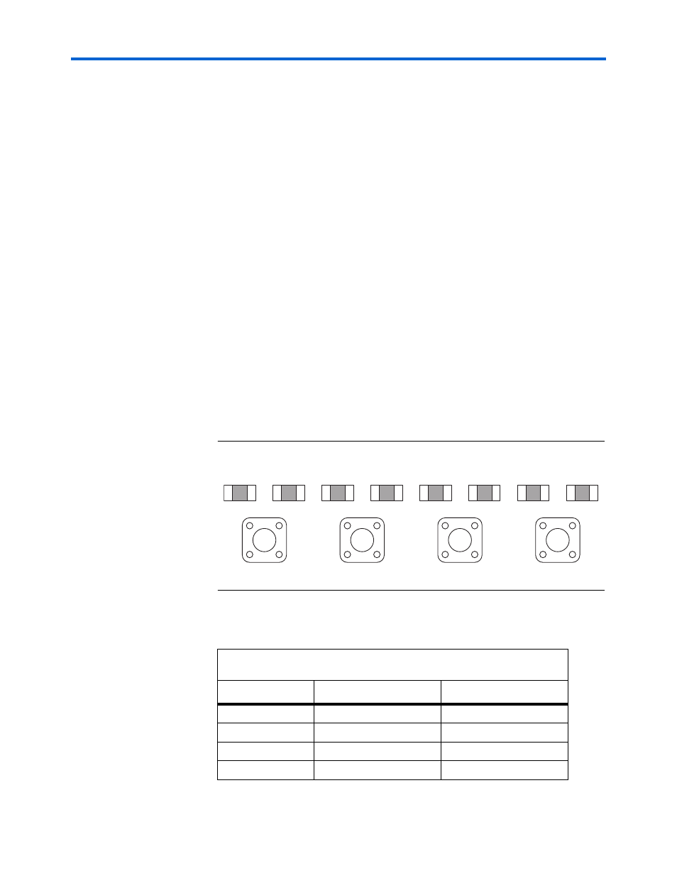
Push-Button
Switches (SW0 -
SW3)
SW0 – SW3 are momentary-contact push-button switches to provide
stimulus to designs in the FPGA. Refer to
. Each switch is
connected to an FPGA general-purpose I/O pin with a pull-up resistor as
shown in
. Each I/O pin perceives a logic 0 when its
corresponding switch is pressed.
Figure 2–2. Push-Button Switches (SW0 – SW3)
Table 2–3. Push Button Switches Pin Table
Button
FPGA Pin
Board Net Name
SW0
Y11
user_pb0
SW1
AA10
user_pb1
SW2
AB10
user_pb2
SW3
AE6
user_pb3
SW0
D0
D1
SW1
D2
D3
SW2
D4
D5
SW3
D6
D7