Serial connector (j19), Serial connector (j19) –15 – Altera Nios Development Board Cyclone II Edition User Manual
Page 27
Altera Corporation
Reference Manual
2–15
May 2007
Nios Development Board Cyclone II Edition
Board Components
f
See www.smsc.com for detailed information about the LAN91C111
device.
Serial Connector
(J19)
J19 is a standard DB-9 serial connector, and is typically used for
communication between the FPGA and a host computer via an RS-232
serial cable. Level-shifting buffer (U52) is used between J19 and the
FPGA, because the FPGA device cannot interface to RS-232 voltage levels
directly.
J19 is able to transmit all RS-232 signals. Alternately, the FPGA design can
use only the signals it needs, such as J19’s RXD and TXD pins. LEDs are
connected to the RXD and TXD signals and visually indicate when data
is being transmitted or received.
Figure 6
show the pin
connections between the serial connectors and the FPGA.
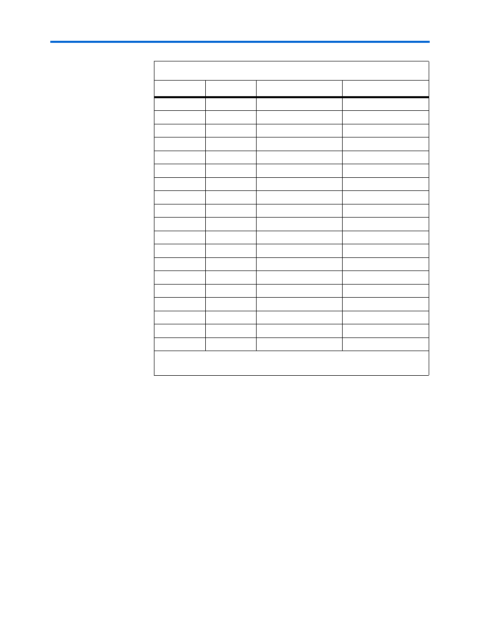
A9
70
Data Line
fe_d13
C10
69
Data Line
fe_d14
D10
68
Data Line
fe_d15
B10
66
Data Line
fe_d16
A10
65
Data Line
fe_d17
E12
64
Data Line
fe_d18
D12
63
Data Line
fe_d19
J13
61
Data Line
fe_d20
J14
60
Data Line
fe_d21
F12
59
Data Line
fe_d22
G12
58
Data Line
fe_d23
J10
56
Data Line
fe_d24
J11
55
Data Line
fe_d25
C11
54
Data Line
fe_d26
B11
53
Data Line
fe_d27
C12
51
Data Line
fe_d28
B12
50
Data Line
fe_d29
D6
49
Data Line
fe_d30
G11
48
Data Line
fe_d31
Note to
:
(1)
Nets fe_a0 and fe_a16 to fe_a23 do not connect to U4.
Table 2–9. Ethernet MAC/PHY Pin Table (Continued)
FPGA Pin
U4 Pin
Pin Function
Board Net Name
(1)