Jtag connector to epm7256ae device (j5), Clock circuitry, Clock circuitry –41 – Altera Nios Development Board Cyclone II Edition User Manual
Page 53
Altera Corporation
Reference Manual
2–41
May 2007
Nios Development Board Cyclone II Edition
Board Components
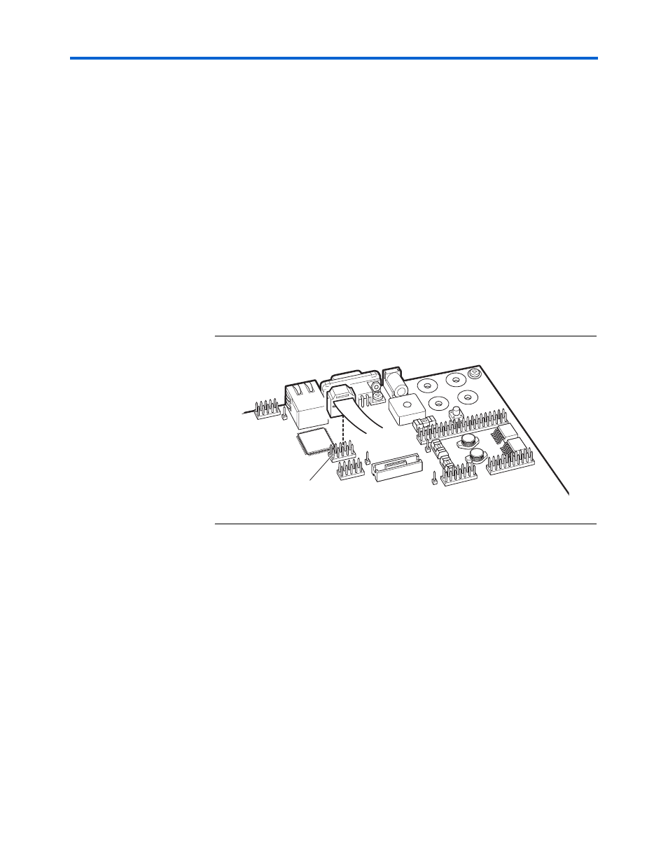
JTAG Connector to EPM7256AE Device (J5)
J5 connects to the JTAG pins (TCK, TDI, TDO, TMS, TRST) of the
EPM7256AE device (U3). Altera Quartus II software can perform in-
system programming (ISP) to reprogram the EPM7256AE device (U3)
with a new hardware image via an Altera download cable as shown in
1
The orientation of J5 is rotated 180
degrees compared to J24.
Most users never need to reprogram the configuration controller design
in the EMP7256AE device. Reprogramming the configuration controller
can result in an inoperable development board.
f
To restore the board to its factory-programmed condition, see Appendix
B: Restoring the Factory Configuration.
Figure 2–20. JTAG Connector (J5) to MAX Device
Clock Circuitry
The Nios development board includes a 50 MHz free-running oscillator
(Y2) and a zero-skew, point-to-point clock distribution network that
drives the FPGA (U62), the EPM7256AE configuration controller device
(U3), and pins on the PROTO1 & PROTO2 connectors. The zero-skew
buffer (U2) drives the clock distribution network using the free-running
50 MHz clock. Refer to
Pin 1
J5