Ddr sdram chip (u63), Ddr sdram chip (u63) –9 – Altera Nios Development Board Cyclone II Edition User Manual
Page 21
Altera Corporation
Reference Manual
2–9
May 2007
Nios Development Board Cyclone II Edition
Board Components
The following pins on U74 have fixed connections, which restricts the
usable modes of operation:
■
MODE is pulled low to enable Linear Burst
■
ZZ is pulled low to leave the chip enabled
■
GLOBALW_n is pulled high to disable the global write
■
CE2 and CE3_n are wired high and low respectively to be enabled
and to make CE1_n the master chip enable
f
See www.cypress.com for detailed information about the SSRAM chip.
DDR SDRAM
Chip (U63)
U63 is a Micron DDR SDRAM chip. Depending on the board revision, the
part number is MT46V16M16TG or MT46V16M16P-6T. The DDR
SDRAM pins are connected to the FPGA as shown in
. Altera
provides a DDR SDRAM controller that allows a Nios II processor to
access the DDR SDRAM device as a large, linearly-addressable memory.
K9
88
GW_n
ssram_gw_n
E5
89
CLK
sram_clk
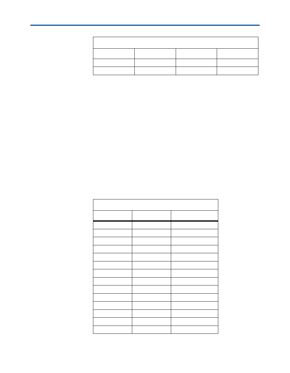
Table 2–6. SSRAM Pin Table (Continued)
FPGA Pin
U74 Pin
Pin Function Board
Net
Name
Table 2–7. DDR SDRAM Pin Table
FPGA Pin
U63 Pin
Board Net Name
R2
2
sdram_dq0
R3
4
sdram_dq1
R4
5
sdram_dq2
P7
7
sdram_dq3
P6
8
sdram_dq4
T2
10
sdram_dq5
T3
11
sdram_dq6
R6
13
sdram_dq7
W2
54
sdram_dq8
W1
56
sdram_dq9
U6
57
sdram_dq10
U7
59
sdram_dq11
U5
60
sdram_dq12
Y1
62
sdram_dq13