Altera Stratix II EP2S180 DSP Development Board User Manual
Page 18
2–10
Core Version a.b.c variable
Altera Corporation
Stratix II EP2S180 DSP Development Board Reference Manual
Functional Description
The Stratix II EP2S180 DSP development board can obtain a clock source
from one or more of the following sources:
■
The on-board crystal oscillator
■
An external clock (through an SMA connector or a Stratix II pin)
The board can provide independent clocks from both the enhanced and
fast PLLs to the A/D converters, the D/A converters, and the other
components that require stable clock sources.
To implement this concept, the enhanced PLL5-dedicated pins drive the
A/D converters and associated functions, and the enhanced
PLL6-dedicated pins drive the D/A converters and associated functions.
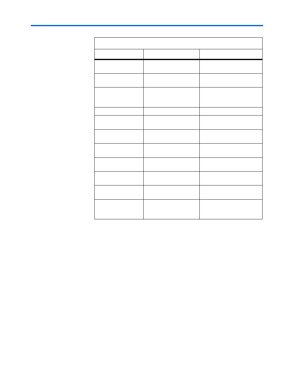
pld_CLKIN0,pld_CLK
IN1
100-MHz oscillator
Stratix II device pins AM17
and A16
pld_CLKIN0_n,pld_C
LKIN1_n
External CLKIN_n input
(J11)
Stratix II device pins AL17
and B16
proto1_OSC,
proto2_OSC
100-MHz oscillator
PROTO1 (J25 pin 9) and
PROTO2 (J28 pin 9) via a
buffer (U7)
cpld_CLKOSC
100-MHz oscillator
CPLD (U10 pin 125)
adc_CLK_IN1,
adc_CLK_IN2
100-MHz oscillator
ADC A (U1 pins 8, 7) and B
(U2 pins 8, 7)
(1)
dac_CLKIN1,
dac_CLKIN2
100-MHz oscillator
DAC A (U14 pin 28) and B
(U15 pin 28)
pld_CLKFB
pld_CLKOUT signal from
the Stratix II pin J14
Stratix II device pin U1
adc_CLK_IN1_n,
adc_CLK_IN2_n
External CLKIN_n input
(J11)
ADC A (U1 pins 8, 7) and B
(U2 pins 8, 7)
(1)
dac_DACCLKIN1,
dac_DACCLKIN2
External DA_EXT_CLK
input (J12)
DAC A (U14 pin 28) and B
(U15 pin 28)
pld_DACCLKIN
External DA_EXT_CLK
input (J12)
Stratix II device pin E16
proto1_CLKOUT,
proto2_CLKOUT
PROTO1 (J25 pin 13)
PROTO2 (J28 pin 13) via
a buffer (U7)
Stratix II device pins T32 and
T30
Notes to
:
(1)
J3 and J4 control which clock is routed to the A/D converters. See
Table 2–10
for
details.
(2)
J18 and J19 control which clock is routed to the D/A converters. See
for details.
Table 2–4. Clock Distribution Signals (Part 2 of 2)
Signal Name
Comes From
Goes To