Altera Stratix II EP2S180 DSP Development Board User Manual
Page 58
2–50
Core Version a.b.c variable
Altera Corporation
Stratix II EP2S180 DSP Development Board Reference Manual
Expansion Interfaces
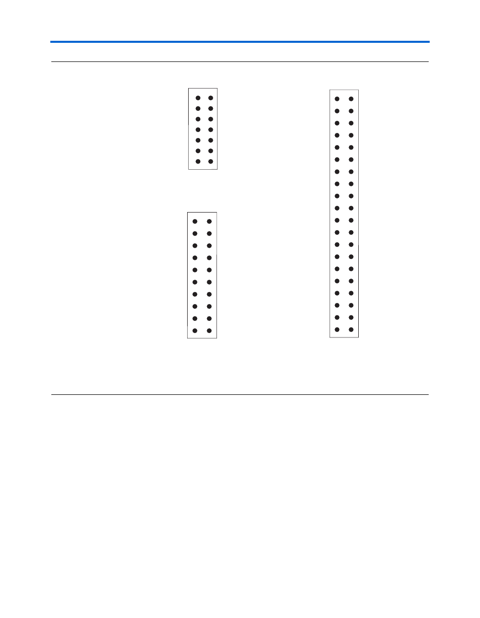
Figure 2–13. Expansion Prototype Connector -Pin Information for J26, J27, & J28
Notes to
Figure 2–13
:
(1)
Unregulated voltage from AC to DC power transformer
(2)
Clk from board oscillator
(3)
Clk from the Stratix II device via buffer
(4)
Clk output from card connected to the Stratix II device.
RESET_n
AC27
AD27
Y23
Y25
AA27
Y27
W25
W27
GND
W29
W28
V24
V23
V28
U28
U23
U22
M23
M22
GND
AC26
AD26
Y22
Y24
AA26
Y26
W24
W26
NC
GND
GND
GND
V29
GND
U27
NC
L25
AF19
GND
1
3
5
7
9
11
13
15
17
19
21
23
25
27
29
31
33
35
37
39
2
4
6
8
10
12
14
16
18
20
22
24
26
28
30
32
34
36
38
40
J26
J27
(1) Vunreg (U54 pin 2)
NC
+3.3V
+3.3V
(2) PROTO2_OSC(U2 pin 6)
(3) PROTO2_CLKIN (U2 pin 17)
(4) PROTO2_CLKOUT (B14)
+3.3V
+3.3V
+3.3V
GND
GND
GND
GND
GND
GND
GND
GND
GND
GND
1
3
5
7
9
11
13
15
17
19
2
4
6
8
10
12
14
16
18
20
GND
AJ17
K26
L23
J26
H27
K24
+V5
K27
L24
J27
H28
K25
AK17
1
3
5
7
9
11
13
2
4
6
8
10
12
14
J28