Altera Stratix II EP2S180 DSP Development Board User Manual
Page 43
Altera Corporation
Core Version a.b.c variable
2–35
Stratix II EP2S180 DSP Development Board Reference Manual
Board Components & Interfaces
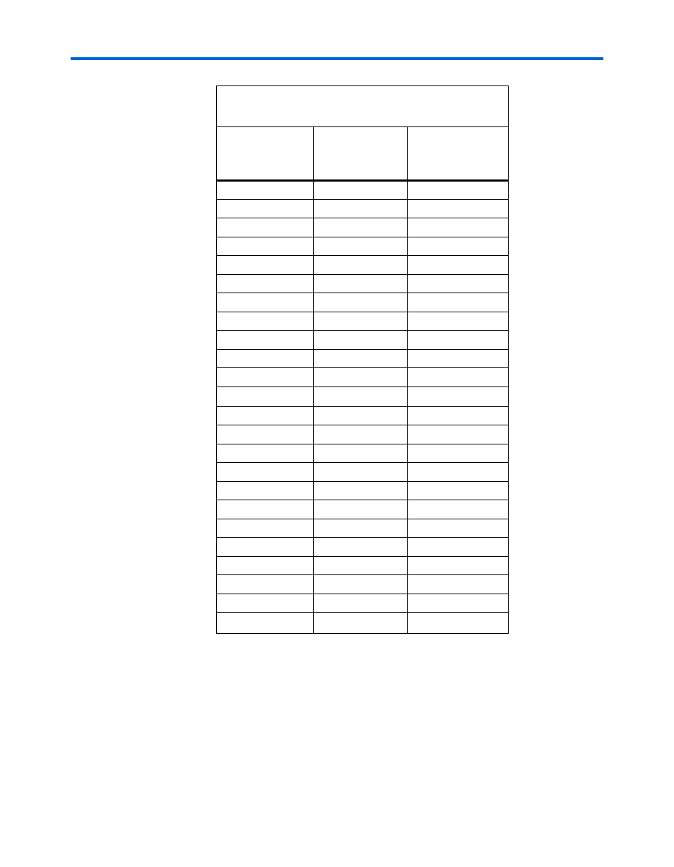
27
D11
AA2
28
D12
AA4
29
D13
Y5
30
D14
AB2
31
D15
AB4
32
CS1#
AC9
33
VS1#
AB10
34
IORD#
AC2
35
IOWR#
AC1
36
WE#
AC6
37
INTRQ
AC4
38
VCC
V
CC
(2)
39
CSEL#
AC8
40
VS2# AB9
41
RESET
AE12
42
WAIT#
AC3
43
INPACK#
AC7
44
REG#
AB7
45
DASP#
AE4
46
PDIAG#
AF2
47
DO8
V3
48
DO9
W2
49
D10
Y3
50
VSS
GND
(3)
Notes to
Table 2–28
:
(1)
All pin numbers represent I/O pins on the FPGA, unless
otherwise noted.
(2)
This FPGA I/O pin controls a power MOSFET that supplies
5V V
CC
to CON1.
(3)
This pin does not connect to the FPGA directly.
(4)
RESET is driven by the EPM7256AE configuration
controller device.
Table 2–28. CompactFlash (CON1) Pin Table (Part 2
of 2)
Pin on
CompactFlash
(CON1)
CompactFlash
Function (U60)
Connects to
(1)