Altera Stratix II EP2S180 DSP Development Board User Manual
Page 25
Altera Corporation
Core Version a.b.c variable
2–17
Stratix II EP2S180 DSP Development Board Reference Manual
Board Components & Interfaces
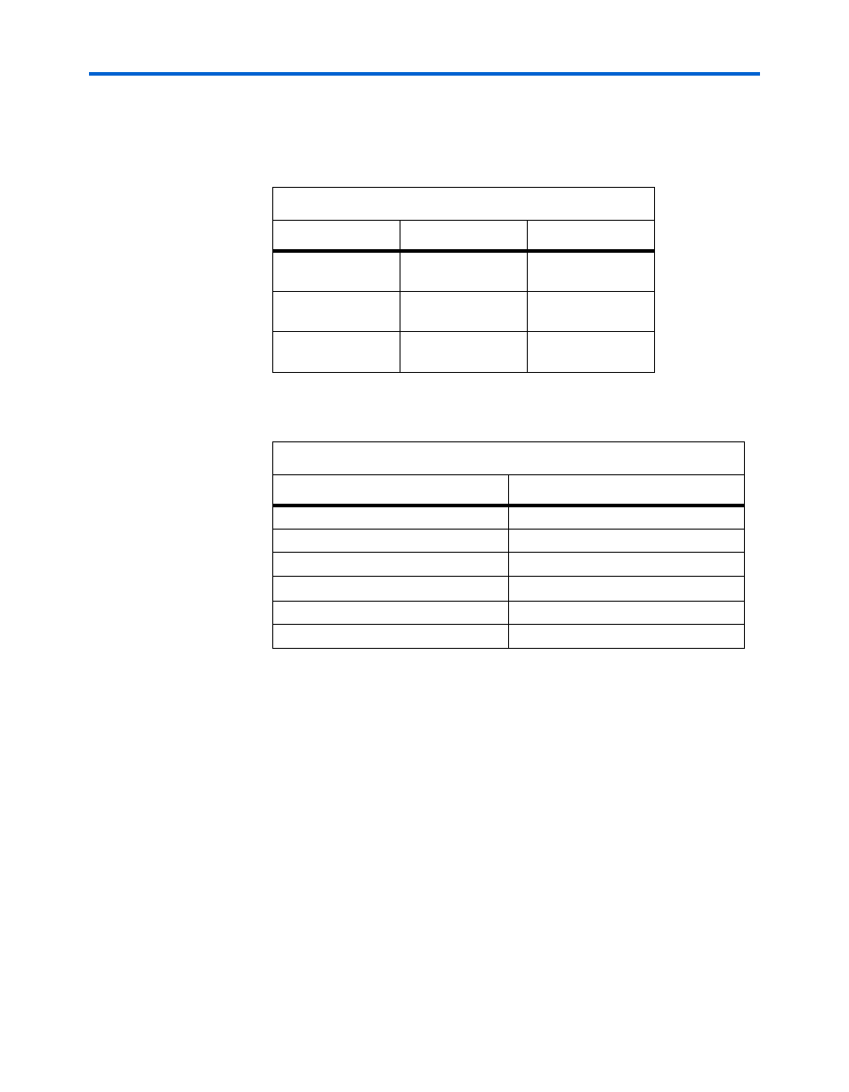
to select the clock for ADC B.
Table 2–10
explains how to select these three
clock signals. The selected clock will pass through a differential LVPECL
buffer before arriving at the clock input to both A/D converters
Table 2–11
lists reference information for the A/D converters.
Table 2–10. A/D Clock Source Settings
J3, J4 Setting
Clock Source
Signal Name
Pins 1 and 2
Stratix II PLL
circuitry
adc_PLLCLK1,
adc_PLLCLK2
Pins 3 and 4
OSC or External
input clock positive
adc_CLK_IN1,
adc_CLK_IN2
Pins 5 and 6
OSC or External
input clock negative
adc_CLK_IN1_n,
adc_CLK_IN2_n
Table 2–11. A/D Converter Reference
Item
Description
Board reference
U1, U2
Part number
AD9433BSQ
Device description
12-bit, 125-MSPS A/D converter
Voltage
3.3-V digital V
DD
, 5.0-V analog V
DD
Manufacturer
Analog Devices
Manufacturer web site
www.analog.com