Chapter 3 – DFI BT968 User Manual
Page 22
www.dfi .com
Chapter 3 Hardware Installation
22
Chapter 3
Signal
Pin#
Module Pin Type Pwr Rail /Tolerance
BT968
Carrier Board
Description
SPI_CS#
B97
O CMOS
3.3V Suspend/3.3V
Connect a series resistor 33ȟ to Carrier Board SPI Device CS# pin
Chip select for Carrier Board SPI - may be sourced from chipset SPI0 or SPI1
SPI_MISO
A92
I CMOS
3.3V Suspend/3.3V
Connect a series resistor 33ȟ to Carrier Board SPI Device SO pin
Data in to Module from Carrier SPI
SPI_MOSI
A95
O CMOS
3.3V Suspend/3.3V
Connect a series resistor 33ȟ to Carrier Board SPI Device SI pin
Data out from Module to Carrier SPI
SPI_CLK
A94
O CMOS
3.3V Suspend/3.3V
Connect a series resistor 33ȟ to Carrier Board SPI Device SCK pin
Clock from Module to Carrier SPI
SPI_POWER
A91
O
3.3V Suspend/3.3V
Power supply for Carrier Board SPI – sourced from Module – nominally
3.3V. The Module shall provide a minimum of 100mA on SPI_POWER.
Carriers shall use less than 100mA of SPI_POWER. SPI_POWER
shall only be used to power SPI devices on the Carrier
BIOS_DIS0#
A34
BIOS_DIS1#
B88
Signal
Pin#
Module Pin Type Pwr Rail /Tolerance
BT968
Carrier Board
Description
VGA_RED
B89
O Analog
Analog
PD 150R
PD 150R,connect to VGA connector with EMI filter & ESD protect component.
Red for monitor. Analog output
VGA_GRN
B91
O Analog
Analog
PD 150R
PD 150R,connect to VGA connector with EMI filter & ESD protect component.
Green for monitor. Analog output
VGA_BLU
B92
O Analog
Analog
PD 150R
PD 150R,connect to VGA connector with EMI filter & ESD protect component.
Blue for monitor. Analog output
VGA_HSYNC
B93
O CMOS
3.3V / 3.3V
Connect to VGA connector with a3.3V Buffer IC to isolate PCH & Display Device Horizontal sync output to VGA monitor
VGA_VSYNC
B94
O CMOS
3.3V / 3.3V
Connect to VGA connector with a 33V Buffer IC to isolate PCH & Display Device Vertical sync output to VGA monitor
VGA_I2C_CK
B95
I/O OD CMOS
3.3V / 3.3V
PD 2.2K to 3.3V
Connect to VGA connector with a 3.3V to 5V Level shift circuit.
DDC clock line (I2C port dedicated to identify VGA monitor capabilities)
VGA_I2C_DAT
B96
I/O OD CMOS
3.3V / 3.3V
PD 2.2K to 3.3V
Connect to VGA connector with a 3.3V to 5V Level shift circuit.
DDC data line.
Signal
Pin#
Module Pin Type Pwr Rail /Tolerance
BT968
Carrier Board
Description
SER0_TX
A98
O CMOS
3.3V/5V
PD 4.7K
General purpose serial port 0 transmitter
(Recommend add Protecting Logic Level Signals on Pins Reclaimed from VCC_12V)
SER0_RX
A99
I CMOS
3.3V/5V
PU 47K to 3.3V
General purpose serial port 0 receiver
(Recommend add Protecting Logic Level Signals on Pins Reclaimed from VCC_12V)
SER1_TX
A101
O CMOS
3.3V/5V
PD 4.7K
General purpose serial port 1 transmitter
(Recommend add Protecting Logic Level Signals on Pins Reclaimed from VCC_12V)
SER1_RX
A102
I CMOS
3.3V/5V
PU 47K to 3.3V
General purpose serial port 1 receiver
(Recommend add Protecting Logic Level Signals on Pins Reclaimed from VCC_12V)
Signal
Pin#
Module Pin Type Pwr Rail /Tolerance
BT968
Carrier Board
Description
I2C_CK
B33
I/O OD CMOS
3.3V Suspend/3.3V
PU 2.2K to 3.3VSB
General purpose I2C port clock output
I2C_DAT
B34
I/O OD CMOS
3.3V Suspend/3.3V
PU 2.2K to 3.3VSB
General purpose I2C port data I/O line
SPKR
B32
O CMOS
3.3V / 3.3V
Output for audio enunciator - the "speaker" in PC-AT systems.
This port provides the PC beep signal and is mostly intended for
debugging purposes.
WDT
B27
O CMOS
3.3V / 3.3V
Output indicating that a watchdog time-out event has occurred.
FAN_PWNOUT
B101
O OD CMOS
3.3V / 3.3V
Fan speed control. Uses the Pulse Width Modulation (PWM) technique to control the fan's RPM.
(Recommend add Protecting Logic Level Signals on Pins Reclaimed from VCC_12V)
FAN_TACHIN
B102
I OD CMOS
3.3V / 3.3V
Fan tachometer input for a fan with a two pulse output.
(Recommend add Protecting Logic Level Signals on Pins Reclaimed from VCC_12V)
TPM_PP
A96
I CMOS
3.3V / 3.3V
PD 10K
Trusted Platform Module (TPM) Physical Presence pin. Active high.
TPM chip has an internal pull down. This signal is used to indicate
Physical Presence to the TPM.
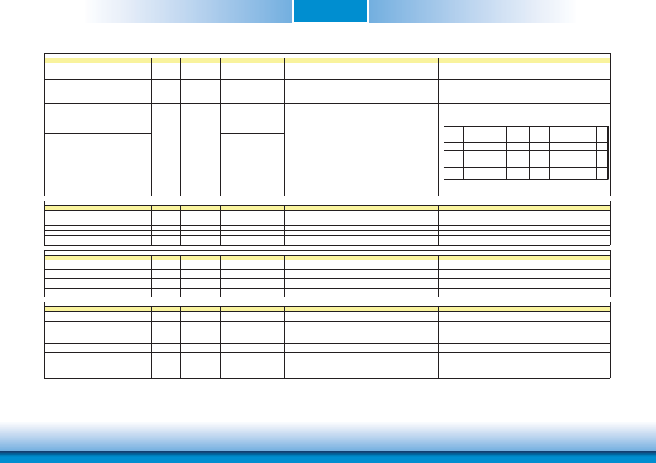
SPI Signals Descriptions
VGA Signals Descriptions
NA
Selection straps to determine the BIOS boot device.
The Carrier should only float these or pull them low, please refer to
COM Express Module Base Specification Revision 2.1 for strapping options of BIOS disable signals.
Serial Interface Signals Descriptions
Miscellaneous Signal Descriptions
I CMOS
Ref
Line
Bios
Entry
SPI
Descriptor
Carrier
SPI_CS#
Chipset
SPI CS0#
Destination
Chipset
SPI CS1#
Destination
BIOS
DIS0#
BIOS
DIS1#
1
1
1
1
0
0
0
0
Module
Module
SPI0/SPI1
SPI1
(Default)
SPI0
High
High
Carrier
Carrier
Carrier
(Default)
Module
(Default)
Module
Module
Module
(Default)
Module
Module
Module
3
2
1
0
Carrier FWH
SPI0/SPI1
(Default)
SPI0/SPI1