Chapter 3 – DFI HM920-HM86 User Manual
Page 20
www.dfi .com
Chapter 3 Hardware Installation
20
Chapter 3
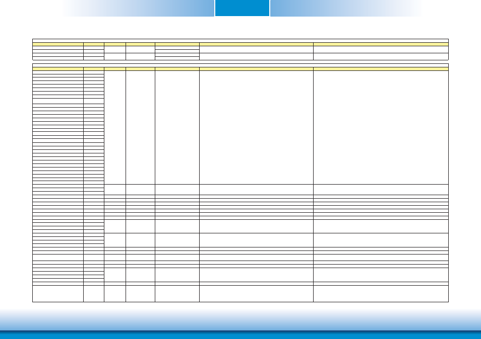
Signal
Pin#
Module Pin Type Pwr Rail /Tolerance
HM920
Carrier Board
Description
EXCD0_CPPE#
A49
PU 10k to 3.3V
EXCD1_CPPE#
B48
PU 10k to 3.3V
EXCD0_PERST#
A48
EXCD1_PERST#
B47
Signal
Pin#
Module Pin Type Pwr Rail /Tolerance
HM920
Carrier Board
Description
PCI_AD0
C24
PCI_AD1
D22
PCI_AD2
C25
PCI_AD3
D23
PCI_AD4
C26
PCI_AD5
D24
PCI_AD6
C27
PCI_AD7
D25
PCI_AD8
C28
PCI_AD9
D27
PCI_AD10
C29
PCI_AD11
D28
PCI_AD12
C30
PCI_AD13
D29
PCI_AD14
C32
PCI_AD15
D30
PCI_AD16
D37
PCI_AD17
C39
PCI_AD18
D38
PCI_AD19
C40
PCI_AD20
D39
PCI_AD21
C42
PCI_AD22
D40
PCI_AD23
C43
PCI_AD24
D42
PCI_AD25
C45
PCI_AD26
D43
PCI_AD27
C46
PCI_AD28
D44
PCI_AD29
C47
PCI_AD30
D45
PCI_AD31
C48
PCI_CBE0-
D26
PCI_CBE1-
C33
PCI_CBE2-
C38
PCI_DEVSEL#
C36
I/O CMOS
3.3V / 5V
PU 8.2K TO 3.3V
PCI bus Device Select, active low.
PCI_FRAME#
D36
I/O CMOS
3.3V / 5V
PU 8.2K TO 3.3V
PCI bus Frame control line, active low.
PCI_IRDY#
C37
I/O CMOS
3.3V / 5V
PU 8.2K TO 3.3V
PCI bus Initiator Ready control line, active low.
PCI_TRDY#
D35
I/O CMOS
3.3V / 5V
PU 8.2K TO 3.3V
PCI bus Target Ready control line, active low.
PCI_STOP#
D34
I/O CMOS
3.3V / 5V
PU 8.2K TO 3.3V
PCI bus STOP control line, active low, driven by cycle initiator.
PCI_PAR
D32
I/O CMOS
3.3V / 5V
PCI bus parity
PCI_PERR#
C34
I/O CMOS
3.3V / 5V
PU 8.2K TO 3.3V
Parity Error: An external PCI device drives PERR# when it receives data that has a parity error.
PCI_REQ0-
C22
PCI_REQ1-
C19
PCI_REQ2-
C17
PCI_REQ3-
D20
P_GNT_0-
C20
P_GNT_1-
C18
P_GNT_2-
C16
P_GNT_3-
D19
PCI_RESET#
C23
O CMOS
3.3V Suspend/ 5V
PCI Reset output, active low.
PCI_LOCK#
C35
I/O CMOS
3.3V / 5V
PU 8.2K TO 3.3V
PCI Lock control line, active low.
PCI_SERR#
D33
I/O OD CMOS
3.3V / 5V
PU 8.2K TO 3.3V
System Error: SERR# may be pulsed active by any PCI device that
detects a system error condition.
PCI_PME#
C15
I CMOS
3.3V Suspend/ 5V
PU 10K TO 3.3VSB
PCI Power Management Event: PCI peripherals drive PME# to wake system from low-power states S1–S5.
PCI_CLKRUN#
D48
I/O CMOS
3.3V / 5V
PU 8.2K TO 3.3V
Bidirectional pin used to support PCI clock run protocol for mobile systems.
PCI_IRQA#
C49
PCI_IRQB#
C50
PCI_IRQC#
D46
PCI_IRQD#
D47
PCI_CLK
D50
O CMOS
3.3V / 3.3V
PCI 33MHz clock output.
PCI_M66EN
D49
I CMOS
3.3V / 5V
Module input signal indicates whether an off-Module PCI device is capable of 66MHz operation. Pulled to
GND by Carrier Board device or by Slot Card if the devices are NOT capable of 66 MHz operation.
If the Module is not capable of supporting 66 MHz PCI operation, this input may be a no-connect on the
Module.
If the Module is capable of supporting 66 MHz PCI operation, and if this input is held low by the Carrier
ȟ
ȟ
ȟ
ȟ
PCI Signals Descriptions
O CMOS
3.3V /3.3V
PCI ExpressCard: reset, active low, one per card
ExpressCard Signals Descriptions
I CMOS
3.3V /3.3V
PCI ExpressCard: PCI Express capable card request, active low, one per
card
I/O CMOS
3.3V /5V
PCI bus multiplexed address and data lines
I/O CMOS
3.3V /5V
PCI bus byte enable lines, active low
PCI bus master request input lines, active low.
PCI bus master grant output lines, active low.
PCI interrupt request lines.
I CMOS
3.3V / 5V
PU 8.2K TO 3.3V
O CMOS
3.3V / 5V
I CMOS
3.3V / 5V
PU 8.2K TO 3.3V