Chapter 3 – DFI HM920-HM86 User Manual
Page 21
www.dfi .com
Chapter 3 Hardware Installation
21
Chapter 3
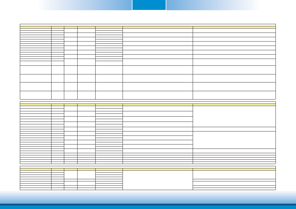
Signal
Pin#
Module Pin Type Pwr Rail /Tolerance
HM920
Carrier Board
Description
USB0+
A46
USB0-
A45
USB1+
B46
USB1-
B45
USB2+
A43
USB2-
A42
USB3+
B43
USB3-
B42
USB4+
A40
USB4-
A39
USB5+
B40
USB5-
B39
USB6+
A37
USB6-
A36
USB7+
B37
USB7-
B36
USB_0_1_OC#
B44
I CMOS
3.3V Suspend/3.3V
PU 10k to 3.3VSB
Connect to Overcurrent of USB Power Switch
USB over-current sense, USB channels 0 and 1. A pull-up for this line
shall be present on the Module. An open drain driver from a USB
current monitor on the Carrier Board may drive this line low. Do not
pull this line high on the Carrier Board.
USB_2_3_OC#
A44
I CMOS
3.3V Suspend/3.3V
PU 10k to 3.3VSB
Connect to Overcurrent of USB Power Switch
USB over-current sense, USB channels 2 and 3. A pull-up for this line
shall be present on the Module. An open drain driver from a USB
current monitor on the Carrier Board may drive this line low. Do not
pull this line high on the Carrier Board.
USB_4_5_OC#
B38
I CMOS
3.3V Suspend/3.3V
PU 10k to 3.3VSB
Connect to Overcurrent of USB Power Switch
USB over-current sense, USB channels 4 and 5. A pull-up for this line
shall be present on the Module. An open drain driver from a USB
current monitor on the Carrier Board may drive this line low. Do not
pull this line high on the Carrier Board.
USB_6_7_OC#
A38
I CMOS
3.3V Suspend/3.3V
PU 10k to 3.3VSB
Connect to Overcurrent of USB Power Switch
USB over-current sense, USB channels 6 and 7. A pull-up for this line
shall be present on the Module. An open drain driver from a USB
current monitor on the Carrier Board may drive this line low. Do not
pull this line high on the Carrier Board.
Signal
Pin#
Module Pin Type Pwr Rail /Tolerance
HM920
Carrier Board
Description
LVDS_A0+
A71
LVDS_A0-
A72
LVDS_A1+
A73
LVDS_A1-
A74
LVDS_A2+
A75
LVDS_A2-
A76
LVDS_A3+
A78
LVDS_A3-
A79
LVDS_A_CK+
A81
LVDS_A_CK-
A82
LVDS_B0+
B71
LVDS_B0-
B72
LVDS_B1+
B73
LVDS_B1-
B74
LVDS_B2+
B75
LVDS_B2-
B76
LVDS_B3+
B77
LVDS_B3-
B78
LVDS_B_CK+
B81
LVDS_B_CK-
B82
LVDS_VDD_EN
A77
O CMOS
3.3V / 3.3V
PU 10K TO 3.3V
Connect to enable control of LVDS panel power circuit
LVDS panel power enable
LVDS_BKLT_EN
B79
O CMOS
3.3V / 3.3V
Connect to enable control of LVDS panel backlight power circuit.
LVDS panel backlight enable
LVDS_BKLT_CTRL
B83
O CMOS
3.3V / 3.3V
Connect to brightness control of LVDS panel backlight power circuit.
LVDS panel backlight brightness control
LVDS_I2C_CK
A83
I/O OD CMOS
3.3V / 3.3V
PU 4.7K TO 3.3V
Connect to DDC clock of LVDS panel
I2C clock output for LVDS display use
LVDS_I2C_DAT
A84
I/O OD CMOS
3.3V / 3.3V
PU 4.7K TO 3.3V
Connect to DDC data of LVDS panel
I2C data line for LVDS display use
Signal
Pin#
Module Pin Type Pwr Rail /Tolerance
HM920
Carrier Board
Description
LPC_AD0
B4
LPC_AD1
B5
LPC_AD2
B6
LPC_AD3
B7
LPC_FRAME#
B3
O CMOS
3.3V / 3.3V
LPC frame indicates the start of an LPC cycle
LPC_DRQ0#
B8
LPC_DRQ1#
B9
LPC_SERIRQ
A50
I/O CMOS
3.3V / 3.3V
PU 8.2K TO 3.3V
LPC serial interrupt
LPC_CLK
B10
O CMOS
3.3V / 3.3V
LPC clock output - 33MHz nominal
ȟ
ȟ
ȟ
ȟ
3.3V / 3.3V
LPC serial DMA request
LVDS Channel B differential clock
LPC Signals Descriptions
O LVDS
LVDS
Connect to LVDS connector
O LVDS
LVDS
Connect to LVDS connector
I/O CMOS
3.3V / 3.3V
I CMOS
O LVDS
LVDS
LVDS
Connect to LVDS connector
O LVDS
LVDS
LPC multiplexed address, command and data bus
O LVDS
LVDS
Connect to LVDS connector
LVDS Channel B differential pairs
Ther LVDS flat panel differential pairs (LVDS_A[0:3]+/-, LVDS_B[0:3]+/-. LVDS_A_CK+/-,
LVDS_B_CK+/-) shall have 100ƻ terminations across the pairs at the destination. These
terminations may be on the Carrier Board if the Carrier Board implements a LVDS deserializer
on-board
O LVDS
LVDS
Connect to LVDS connector
Connect to LVDS connector
LVDS Channel A differential clock
O LVDS
LVDS
Connect to LVDS connector
Connect to LPC device
I/O USB
3.3V Suspend/3.3V
Connect 90ಳ @100MHz Common Choke in series and ESD suppressors to GND to USB
connector
USB differential pairs 7, USB7 may be configured as a USB client or as a host, or both, at the
Module designer's discretion.(CR901-B default set as a host)
LVDS Signals Descriptions
O LVDS
LVDS
Connect to LVDS connector
LVDS Channel A differential pairs
Ther LVDS flat panel differential pairs (LVDS_A[0:3]+/-, LVDS_B[0:3]+/-. LVDS_A_CK+/-,
LVDS_B_CK+/-) shall have 100ƻ terminations across the pairs at the destination. These
terminations may be on the Carrier Board if the Carrier Board implements a LVDS deserializer
on-board
O LVDS
Connect to LVDS connector
O LVDS
LVDS
Connect to LVDS connector
I/O USB
I/O USB
3.3V Suspend/3.3V
Connect 90ಳ @100MHz Common Choke in series and ESD suppressors to GND to USB
connector
USB differential pairs 2
I/O USB
3.3V Suspend/3.3V
Connect 90ಳ @100MHz Common Choke in series and ESD suppressors to GND to USB
connector
USB differential pairs 1
I/O USB
3.3V Suspend/3.3V
Connect 90ಳ @100MHz Common Choke in series and ESD suppressors to GND to USB
connector
USB differential pairs 6
3.3V Suspend/3.3V
Connect 90ಳ @100MHz Common Choke in series and ESD suppressors to GND to USB
connector
USB differential pairs 4
I/O USB
3.3V Suspend/3.3V
Connect 90ಳ @100MHz Common Choke in series and ESD suppressors to GND to USB
connector
USB differential pairs 3
I/O USB
3.3V Suspend/3.3V
Connect 90ಳ @100MHz Common Choke in series and ESD suppressors to GND to USB
connector
USB differential pairs 5
USB Signals Descriptions
I/O USB
3.3V Suspend/3.3V
Connect 90ಳ @100MHz Common Choke in series and ESD suppressors to GND to USB
connector
USB differential pairs 0