Reglnamode, Regcompatmode, Regautadd – Linx Technologies TRM-915-R250 User Manual
Page 29: Regnvlnamode, Regnvcompatmode, Regnvautadd
– –
– –
52
53
Compatibility Mode - Address = 0x70; NV Address = 0x25
Compatibility mode allows the 250 Series modules to communicate with
the 25 Series modules. Please see the Compatibility Mode section for more
details. Figure 61 shows examples of the commands and Figure 62 shows
the available values.
Auto Addressing - Address = 0x71; NV Address = 0x26
When this register is enabled, the module reads the Source Address from
a received packet and uses it to fill the Destination Address registers.
This makes sure that a response is sent to the device that transmitted the
original message.
The non-volatile register only uses the lower 4 bits to configure the
automatic addressing. The upper 4 bits are not used.
The volatile register is split in half with the lower 4 bits configuring the
automatic addressing, the same as the non-volatile register.
The upper 4 bits indicate the type of packet that was last received. This
indication is the same as the Network Mode register setting. These bits
are not used by the module and are only written by the module after
successfully receiving a packet.
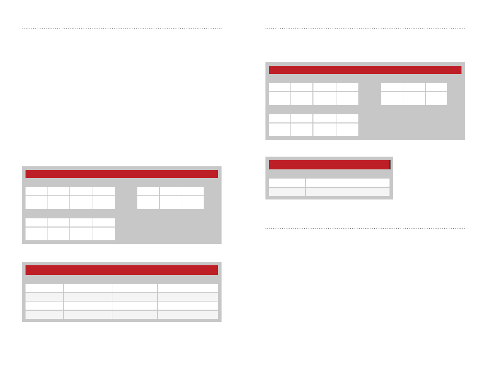
Figure 61: 250 Series Transceiver Compatibility Mode Command and Response
250 Series Compatibility Mode Register Settings
V1
Mode
0x00
Disable Compatibility Mode
0x01
Enable Compatibility Mode
Figure 62: 250 Series Compatibility Mode Register Settings
250 Series Compatibility Mode
Read Command
Read Response
Header
Size
Escape
Address
ACK
Address
Value
0xFF
0x02
0xFE
0x70
0x25
0x06
0x70
0x25
V1
Write Command
Header
Size
Address
Value
0xFF
0x02
0x70
0x25
V1
Receiver LNA Mode - Address = 0x6F; NV Address = 0x24
By default, the module is factory-configured to use its internal Automatic
Gain Control (AGC) circuit to manage receiver sensitivity. Reducing the gain
increases the linearity of the receiver, but reduces maximum sensitivity;
increasing the gain does the opposite. Generally speaking, higher
linearity (increased third order input intercept point, IIP3) gives improved
performance in high-interference environments; high gain yields better
performance in low-interference environments.
The module contains an AGC circuit that manages these settings
automatically, and it should be used whenever possible. When reading the
digital RSSI registers (regIMMEDRSSI, regLGPRSSI), the internal calculation
automatically compensates for the current LNA gain setting. However,
when attempting to make analog RSSI measurements, fixing the LNA gain
produces more meaningful results.
Figure 59 shows examples of the commands and Figure 60 shows the
available values.
250 Series LNA Mode Register Settings
V1
Meaning
IIP3 Increase
Sensitivity Decrease
0x00
AGC Enabled
Variable
Variable
0x01
High Sensitivity
Reference
Reference
0x02
Mid Linearity
19.1dB
6.5dB
0x03
High Linearity
41.8dB
9.5dB
Figure 59: 250 Series Transceiver LNA Mode Command and Response
Figure 60: 250 Series Transceiver LNA Mode Register Settings
250 Series LNA Mode
Read Command
Read Response
Header
Size
Escape
Address
ACK
Address
Value
0xFF
0x02
0xFE
0x6F
0x24
0x06
0x6F
0x24
V1
Write Command
Header
Size
Address
Value
0xFF
0x02
0x6F
0x24
V1