Pin assignments, Pin descriptions – Linx Technologies TRM-915-R250 User Manual
Page 5
– –
– –
4
5
Figure 4: Electrical Specifications
250 Series Transceiver Specifications
Parameter
Symbol
Min.
Typ.
Max.
Units
Notes
Interface Section
Input Logic Low
V
I L
0
0.8
VDC
Input Logic High
V
I H
2.0
V
CC
VDC
Output Logic Low
V
OL
I
OL
= 8.5mA
0.6
VDC
I
OL
= 10µA
0.1
VDC
I
OL
= 25mA
1.0
VDC
Output Logic High
V
OH
I
OH
= -3mA
V
CC
–0.7
VDC
I
OH
= -10µA
V
CC
–0.1
I
OH
= -10mA
V
CC
-0.8
Flash Specifications (Non-Volatile Registers)
Flash Write Duration
16
ms
Flash Write Cycles
20k
100k
cycles
1. V
CC
= 3.3V
2. Into a 50-ohm load
3. At 25ºC
4. 26 channels each
5. At 10
-3
BER
6. P
in
= -20dBm, 2 CW interferers, F
RF
=
915MHz, F
1
= F
RF
+ 3MHz, F
2
= F
RF
+
6MHz, max gain, high-sensitivity
7. Desired signal 3dB above input
sensitivity level, CW interferer power
level increased until BER = 10
-2
,
+/–1MHz
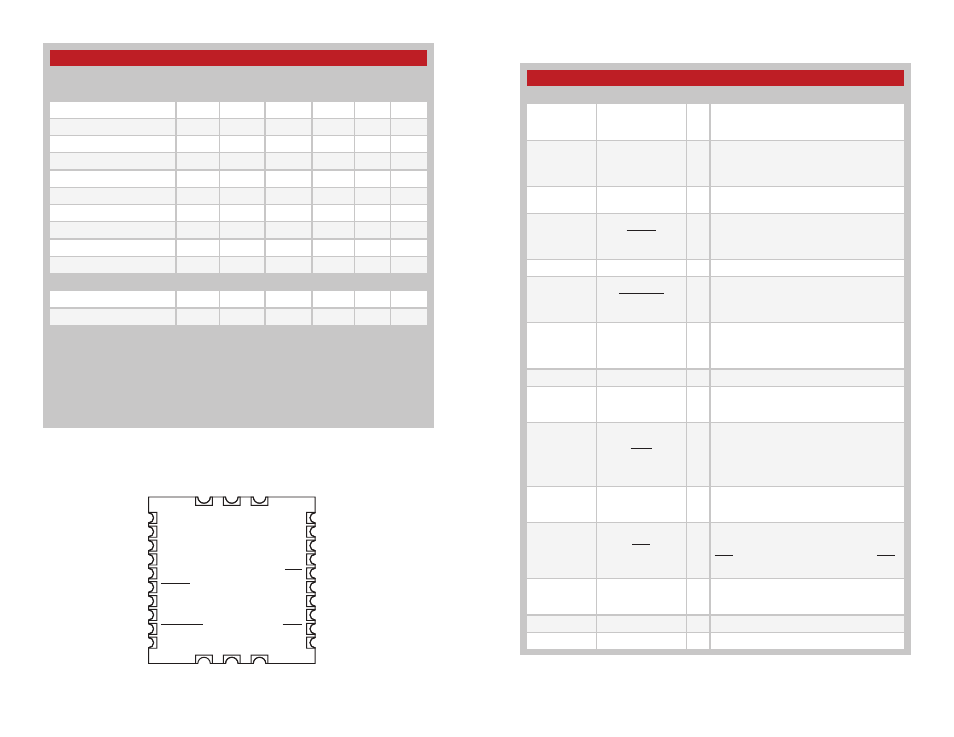
Pin Assignments
1
VCC
2
3
4
6
5
7
8
9
10
26
11
PR_PKT
TXD
NC
NC
EX
CMD_RSP
NC
C2D
RESET
NC
23
22
21
20
18
19
17
16
15
14
GND
ANT
GND
RXD
RSSI
CMD
BE
NC
NC
CTS
12
13
GND
GND
GND
VCC
VCC
25
24
Figure 5: 250 Series Transceiver Pin Assignments (Top View)
Pin Descriptions
Pin Number
Name
I/O Description
1
PR_PKT
O
Processing Packet Indicator. This line goes
high when the module is processing a valid
or potentially valid packet.
2
TXD
O
UART Transmit Data Output. This is the
output line for the configuration command
responses as well as the data received over
the air.
3, 4, 5, 8, 17,
18
NC
—
No Electrical Connection. Do not connect
any traces to these lines.
6
RESET
I/O
Reset line. This line is normally an input that
acts as an active low hardware reset line.
It does occasionally act as an output, so
please see the Reset section for details.
7
C2D
—
Reserved
9
CMD_RSP
O
Command Response. This line is low when
the data on the TXD line is a response to a
command and not data received over the
air.
10
EX
O
Exception Output. A mask can be set
to take this line high when an exception
occurs. The line is lowered when the
exception register is read (regEXCEPTION)
11, 12, 13, 23
GND
—
Ground
14
RSSI
O
This line outputs an analog voltage that is
proportional to the strength of the incoming
signal.
15
CMD
I
Command Input. This line sets the serial
data as either command data to configure
the module or packet data to be sent over
the air. Pull low for command data; pull high
for packet data.
16
BE
O
Buffer Empty. This line goes high when the
UART input buffer is empty, indicating that
all data has been transmitted.
19
CTS
O
UART Clear To Send, active low. This line
indicates to the host microcontroller when
the module is ready to accept data. When
CTS is high, the module is busy. When CTS
is low, the module is ready for data.
20
RXD
I
UART Receive Data Input. This is the input
line for the configuration commands as well
as data to be sent over the air.
22
ANT
—
50-ohm RF Antenna Port
24, 25, 26
VCC
—
Supply Voltage
Figure 6: 250 Series Transceiver Pin Descriptions
Pin Descriptions