A. programming the flash memory device, Cfi flash memory map, Appendix a. programming the flash memory device – Altera Stratix IV GT 100G User Manual
Page 57: Table a–1
October 2010
Altera Corporation
Stratix IV GT 100G Development Kit User Guide
A. Programming the Flash Memory
Device
As you develop your own project using the Altera tools, you can program the flash
memory device so that your own design loads from flash memory into the FPGA on
power up. This appendix describes the preprogrammed contents of the common flash
interface (CFI) flash memory device on the Stratix IV GT 100G development board
and the Nios II EDS tools involved with reprogramming the user portions of the flash
memory device.
The Stratix IV GT 100G development board ships with the CFI flash device
preprogrammed with a default factory FPGA configuration for running the Board
Update Portal design example and a default user configuration for running the Board
Test System demonstration. There are several other factory software files written to
the CFI flash device to support the Board Update Portal. These software files were
created using the Nios II EDS, just as the hardware design was created using the
Quartus II software.
f
For more information about Altera development tools, refer to the
page of the Altera website.
CFI Flash Memory Map
Table A–1
shows the default memory contents of the 128-Mb (1-Gbit) single-die CFI
flash device. For the Board Update Portal to run correctly and update designs in the
user memory, this memory map must not be altered.
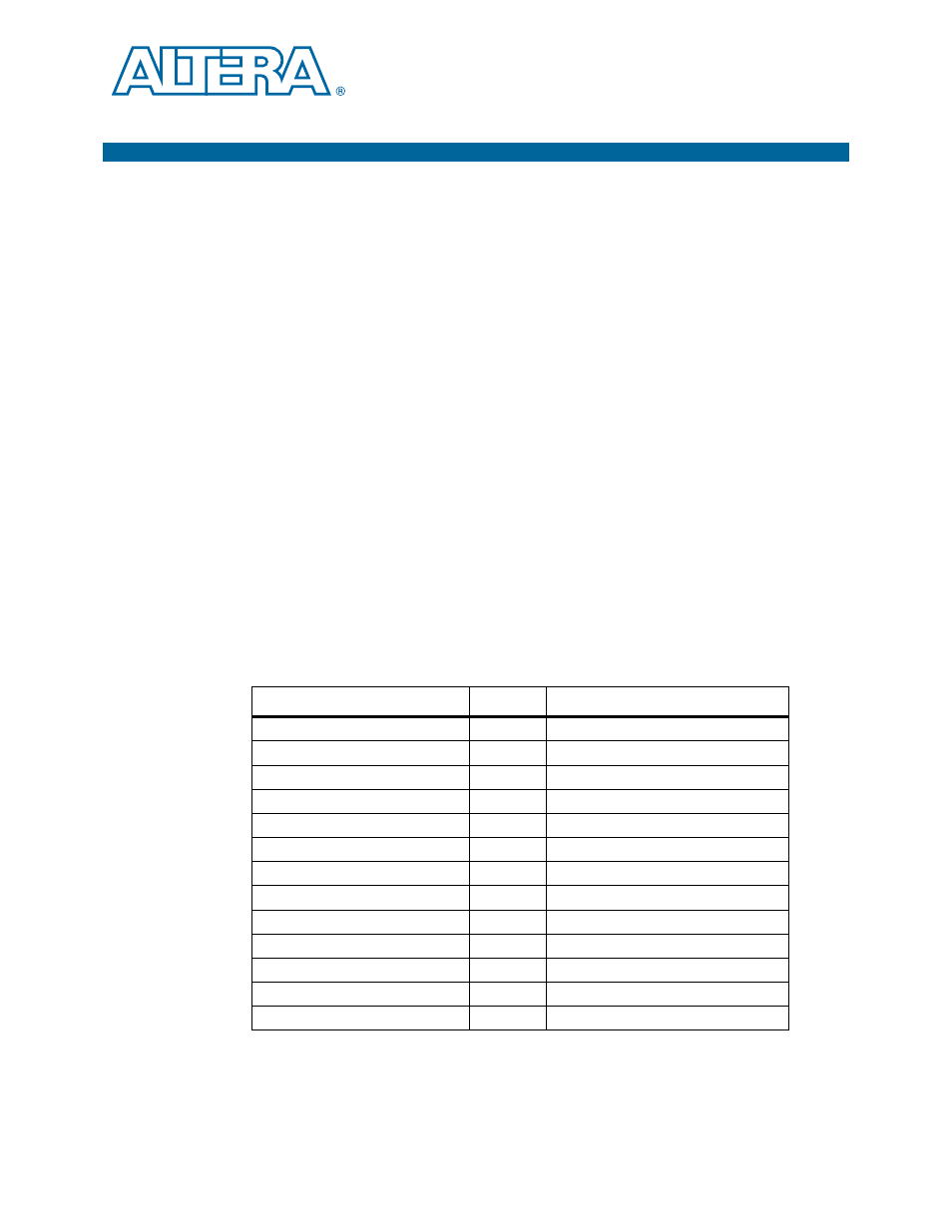
Table A–1. Byte Address Flash Memory Map
Block Description
Size
Address Range
Unused
128 KB
0x07FE0000 - 0x07FFFFFF
User software
26,624 KB
0x065E0000 - 0x07FDFFFF
Factory software
4,096 KB
0x061E0000 - 0x065DFFFF
zipfs (html, web content)
4,096 KB
0x05DE0000 - 0x061DFFFF
User hardware 3
21, 116 KB 0x04940000 - 0x05DDFFFF
User hardware 2
21, 116 KB 0x034A0000 - 0x0493FFFF
User hardware 1
21, 116 KB 0x02000000 - 0x0349FFFF
Reserved
11,136 KB
0x01520000 - 0x01FFFFFF
Factory hardware
21, 116 KB 0x00080000 - 0x0151FFFF
PFL option bits
128 KB
0x00060000 - 0x0007FFFF
Board information
128 KB
0x00040000 - 0x0005FFFF
Ethernet option bits
128 KB
0x00020000 - 0x0003FFFF
User design reset vector
128 KB
0x00000000 - 0x0001FFFF