7 option data and i/o maps – Yaskawa 1000 Series Drive Option - Profibus-DP Installation User Manual
Page 27
7 Option Data and I/O Maps
YASKAWA ELECTRIC TOBP C730600 42C 1000-Series Option SI-P3 Installation Manual
27
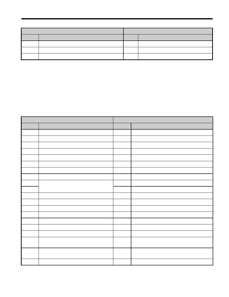
Table 11 Extended Data 1 Register Map
3
Frequency Reference Low Byte
3
Motor Speed Low Byte
4
Torque Reference/Torque Limit High Byte
4
Output Current High Byte
5
Torque Reference/Torque Limit Low Byte
5
Output Current High Byte
<1> Enabled in CLV, AOLV/PM, and CLV/PM control modes (A1-02 = 3, 6, or 7).
<2> Set when network communication is designated as the source of the torque limit and torque reference
(F6-06 = 1). When enabled, d5-01 determines whether the value is read as the torque limit value (d5-01 = 0) or as
the torque reference value (d5-01 = 1). In CLV/PM, this value is read as the torque limit.
<3> Unit depends on the setting of o1-03 (Digital Operator Display Scaling). When the drive is operating in V/f
Control or OLV/PM, the drive output frequency becomes the input data.
<4> Data is displayed in units of 0.01 A for drives 7.5 kW and smaller, and in units of 0.1 A for drives 11 kW and
larger. The number of decimal places in the parameter value depends on the drive model and the ND/HD selection
in parameter C6-01. For delails, refer to the 1.3 Model Number and Nameplate Check of the drive Technical
Manual.
Output (Master Device to Drive)
Input (Drive to Master Device)
Byte
Description
Byte
Description
0
Operation Command High Byte
0
Drive Status High Byte
1
Operation Command Low Byte
1
Drive Status Low Byte
2
Frequency Reference High Byte
2
Motor Speed High Byte
3
Frequency Reference Low Byte
3
Motor Speed Low Byte
4
Torque Reference High Byte
4
Torque Reference Monitor High Byte
5
Torque Reference Low Byte
5
Torque Reference Monitor Low Byte
6
Torque Compensation High Byte
6
Speed Detection PG Pulse Count 1 High Byte
7
Torque Compensation Low Byte
7
Speed Detection PG Pulse Count 1 Low Byte
8
Reserved
8
Frequency Reference High Byte
9
9
Frequency Reference Low Byte
10
Analog Output Channel 1 High Byte
10
Output Frequency High Byte
11
Analog Output Channel 1 Low Byte
11
Output Frequency Low Byte
12
Analog Output Channel 2 High Byte
12
Output Current High Byte
13
Analog Output Channel 2 Low Byte
13
Output Current Low Byte
14
Digital Output High Byte
14
Analog Input Channel 1 High Byte
15
Digital Output Low Byte
15
Analog Input Channel 1 Low Byte
16
MEMOBUS/Modbus Function Code
16
MEMOBUS/Modbus Function Code
17
MEMOBUS/Modbus Starting Register
Address High Byte
17
MEMOBUS/Modbus Starting Register Address
High Byte
18
MEMOBUS/Modbus Starting Register
Address Low Byte
18
MEMOBUS/Modbus Starting Register Address
Low Byte
19
MEMOBUS/Modbus Number of Data
19
MEMOBUS/Modbus Number of Data
Output (Master Device to Drive)
Input (Drive to Master Device)
Byte
Description
Byte
Description