Altera Arria V GT FPGA User Manual
Page 19
Chapter 4: Development Board Setup
4–5
Factory Default Switch and Jumper Settings
November 2012
Altera Corporation
Arria V GT FPGA Development Kit
User Guide
5. Set DIP switch bank (SW8) to match
6. Set the board jumpers to match
and
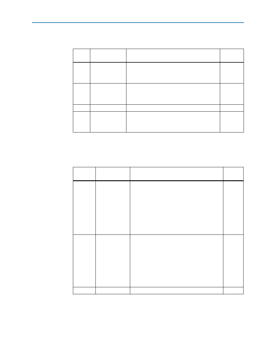
Table 4–5. SW8 FPGA1 MSEL Dip Switch Settings
Switch
Board
Label
Function
Default
Position
1
FPGA1_MSEL[1]
Switch 1 has the following options:
■
When ON, a logic 0 is selected.
■
When OFF, a logic 1 is selected.
ON
2
FPGA1_MSEL[2]
Switch 2 has the following options:
■
When ON, a logic 0 is selected.
■
When OFF, a logic 1 is selected.
OFF
3
—
—
ON
4
FPGA1_MSEL[4]
Switch 4 has the following options:
■
When ON, a logic 0 is selected.
■
When OFF, a logic 1 is selected.
OFF
(1) Ensure that all MSEL setting are in a defined configuration scheme as shown in
e Arria V Device Handbook.
Table 4–6. Jumper Settings (Part 1 of 2)
Board
Reference
Board
Label
Function
Default
Position
J5
FMC_VCCPD
This jumper has the following options:
■
Installing the shunt on pins 1-2 provides 2.5 V on
FMC_VCCPD.
■
Installing the shunt on pins 2-3 provides 3.3 V on
FMC_VCCPD.
c
J5 (VCCPD setting) must be set according the
to voltage supplied by the FMC card to avoid
damaging your development board.
Pins 1-2
J11
FMC_VCCIO_SEL
This jumper has the following options:
■
No shunt = 1.5V
■
Shunt on pins 1-2 = 1.8V
■
Shunt on pins 3-4 = 2.5V
■
Shunt on pins 5-6 = 3.3V
Note: When setting this jumper to 3.3 V, make sure
the FMC_VCCPD is on the correct setting (J5 shunt
on pins 2-3).
Pins 3-4
J14
FAN2
Powers the fan for FPGA 2.
Installed