The system info tab, Board information, Max ii registers – Altera Arria V GT FPGA User Manual
Page 26: The system info tab –4, Board information –4 max ii registers –4
6–4
Chapter 6: Board Test System
Using the Board Test System
Arria V GT FPGA Development Kit
November 2012
Altera Corporation
User Guide
2. On the Configure menu, click the configure command that corresponds to the
functionality you wish to test. The design begins running in the FPGA, and the
corresponding GUI application tabs that interface with the design are now
enabled.
1
If you use the Quartus II Programmer for configuration, rather than the
Board Test System GUI, you may need to restart the GUI.
The System Info Tab
The System Info tab shows the board’s current configuration.
shows the System Info tab. The tab displays the contents of the MAX II registers, the
JTAG chain, the board’s MAC address, and other details stored on the board.
The following sections describe the controls on the System Info tab.
Board Information
The Board information controls display static information about your board.
■
Board Name
—Indicates the official name of the board, given by the Board Test
System.
■
Board P/N
—Indicates the part number of the board.
■
Serial number
—Indicates the serial number of the board.
■
Factory test version
—Indicates the version of the Board Test System currently
running on the board.
■
MAX II ver
—Indicates the version of MAX II code currently running on the board.
The MAX II code resides in the <install
dir>\kits\arriaVGT_5agtfd7kf40_fpga\examples directory. Newer revisions of
this code might be available on the
page of the
Altera website.
■
MAC
—Indicates the MAC address of the board.
MAX II Registers
The MAX II registers control allows you to view and change the current MAX II
register values as described in
. Changes to the register values with the GUI
take effect immediately. For example, writing a 0 to SRST resets the board.
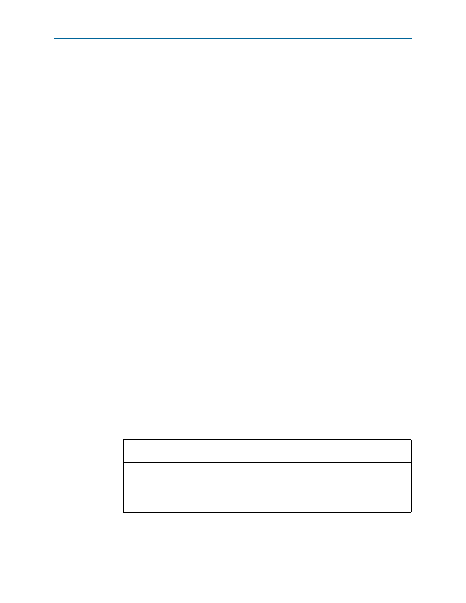
Table 6–1. MAX II Registers (Part 1 of 2)
Register Name
Read/Write
Capability
Description
System Reset
(SRST)
Write only
Set to 0 to initiate an FPGA reconfiguration.
Page Select Register
(PSR)
Read / Write
Determines which of the up to eight (0-7) pages of flash
memory to use for FPGA reconfiguration. The flash memory
ships with pages 0 and 1 preconfigured.