13 clocking scheme, Table 5-1, I2c bus address map – Artesyn XMCspan Installation and Use (June 2014) User Manual
Page 45: Table 5-2, Clocking scheme, Functional description
Functional Description
XMCSPAN Installation and Use (6806800H03C)
45
5.13 Clocking Scheme
A 100 MHz PCI Express reference clock is provided to the XMCspan through expansion
connector pins J3.27 and J3.29.The reference clock is used to generate all other PCI Express
clocks using an ICS9DB108, which is IDT's 8-output differential buffer for PCI Express.
The PCI/PCI-X bus clocks are generated by the Tsi384 internal clock generator. The clock
generator uses REFCLK positive and negative inputs to generate the clock on PCI_CLK0
outputs.The clock frequency is determined by PCI_PCIXCAP, PCI_M66EN, and PCI_SEL100.
The table below lists all the clocks required by the XMCspan, along with their frequency,
source, and clock target device.
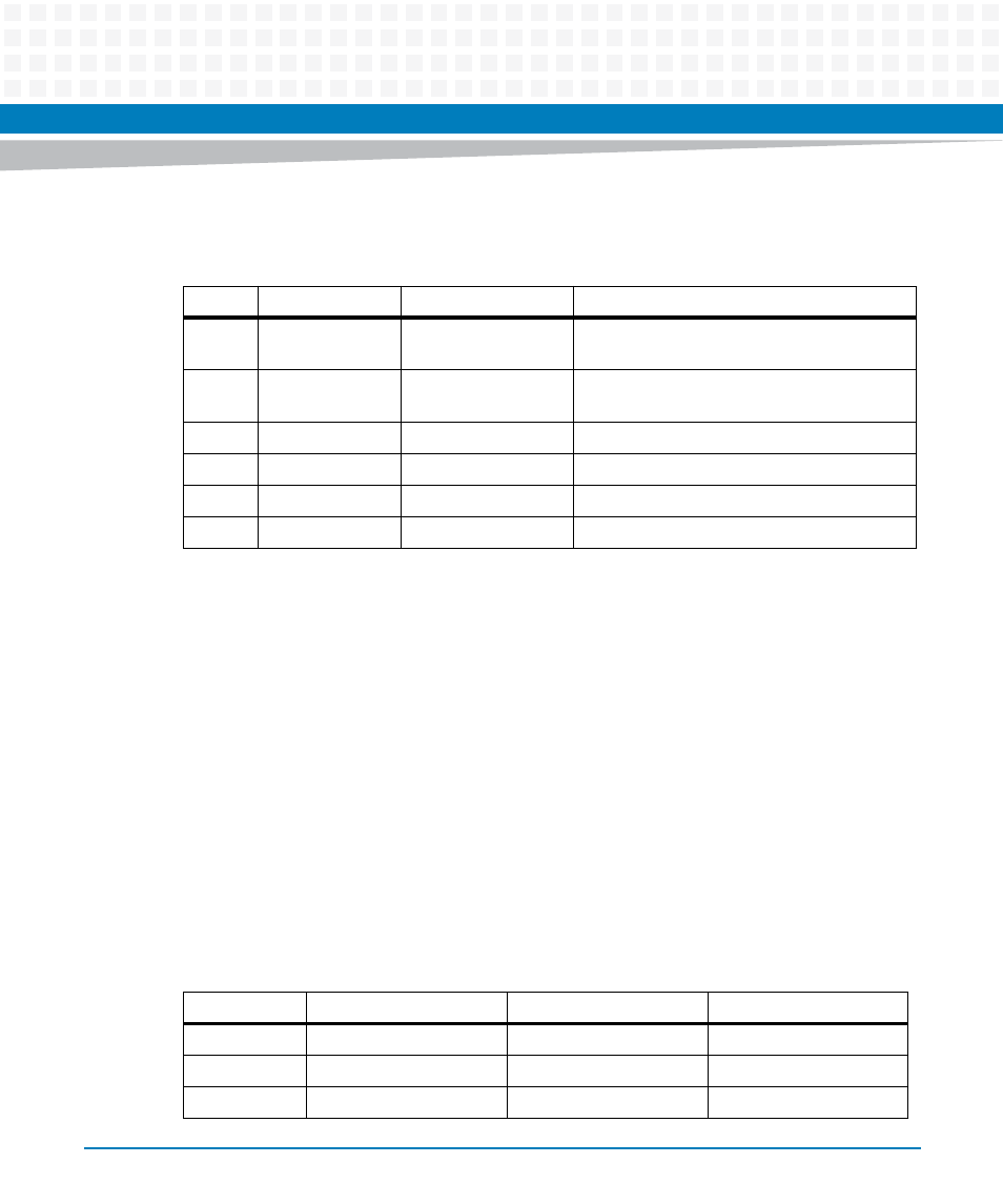
Table 5-1 I2C Bus Address Map
Bus
Address
Size
Function
0
E0x
NA
I2C Bus Multiplexer on the first XMCspan
module
0
E2x
NA
I2C Bus Multiplexer on the first XMCspan
module
1
90x
NA
Temperature Sensor LM75
1
ACx
8 KB
VPD serial EEPROM
2
ACx
-
VPD of XMC module 1
2
AEx
-
VPD of XMC module 2
Table 5-2 Clocking Scheme
Clock Signal
Clock Source
Frequency
Device
CLK_PCI1
Tsi384_1
-
PMC Site 1
CLK_PCI2
Tsi384_2
-
PMC Site 2
CLK_PCIE0
ICS9DB108
100 MHz
PEX8533