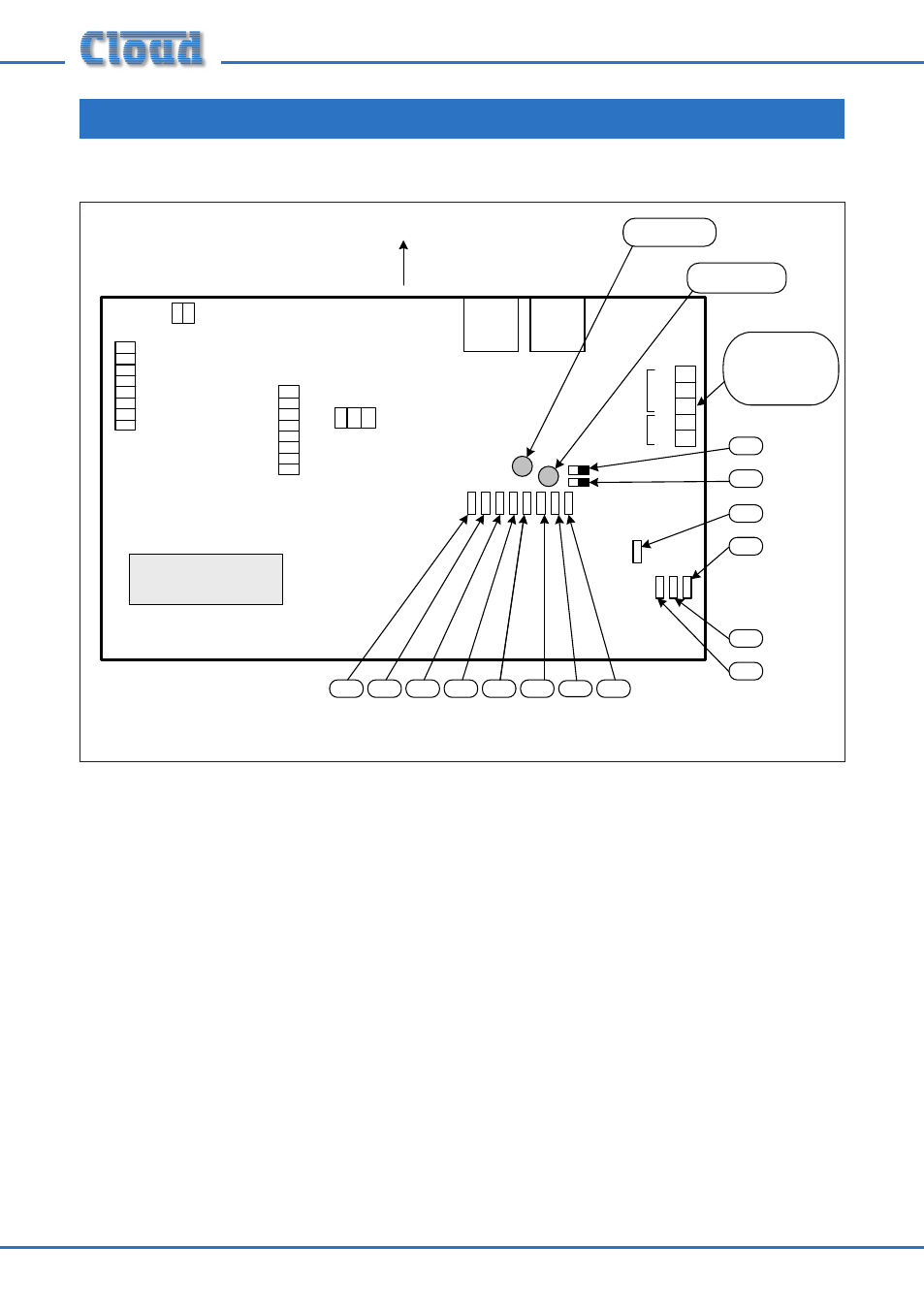
Appendix, Pcb layout diagram – Cloud Electronics PM12 User Manual
Page 32
PM4/8/12/16 Installation and User Guide v2.2
32
Appendix
PCB layout diagram
REAR OF UNIT
CAN PORT
OUT
IN
FLASH MEMORY IC
TERM2
TERM4
TERM1
+ V 0 V
Z1
Z8
Z7
Z6
Z5
Z4
Z3
Z2
Z9
Z16
Z15
Z14
Z13
Z12
Z11
Z10
AUDIO
(TERM8)
H
O
T
C
O
LD
GND
MIC LEVEL
ADJUSTMENT
CHIME LEVEL
ADJUSTMENT
J8
J7
J14
J13
J12
J11
J10
J9
J6
J5
J2
J1
J4
J3
PR2
PR1
PM Jumper Locations
(Illustrative Purposes Only)
HOT
COLD
GND
M
IC
+
-
SP
KR
MIC CAPSULE &
INTERNAL CHIME
SPEAKER
CONNECTOR
When removing jumpers we recommend that the link is left connected to one leg of
the header to prevent loss of the link.
When making internal adjustments please ensure that you:
Disconnect power to the unit before accessing the PCB. If the microphone is
•
powered from another unit, this will mean removing the appropriate connection.
Only reassemble the unit using the original screws.
•