Snubber circuit – Yaskawa GPD 506/P5 Section One User Manual
Page 39
Advertising
PP.P5G5.01.Troubleshoot
Page 39
Rev. 06/11/2003
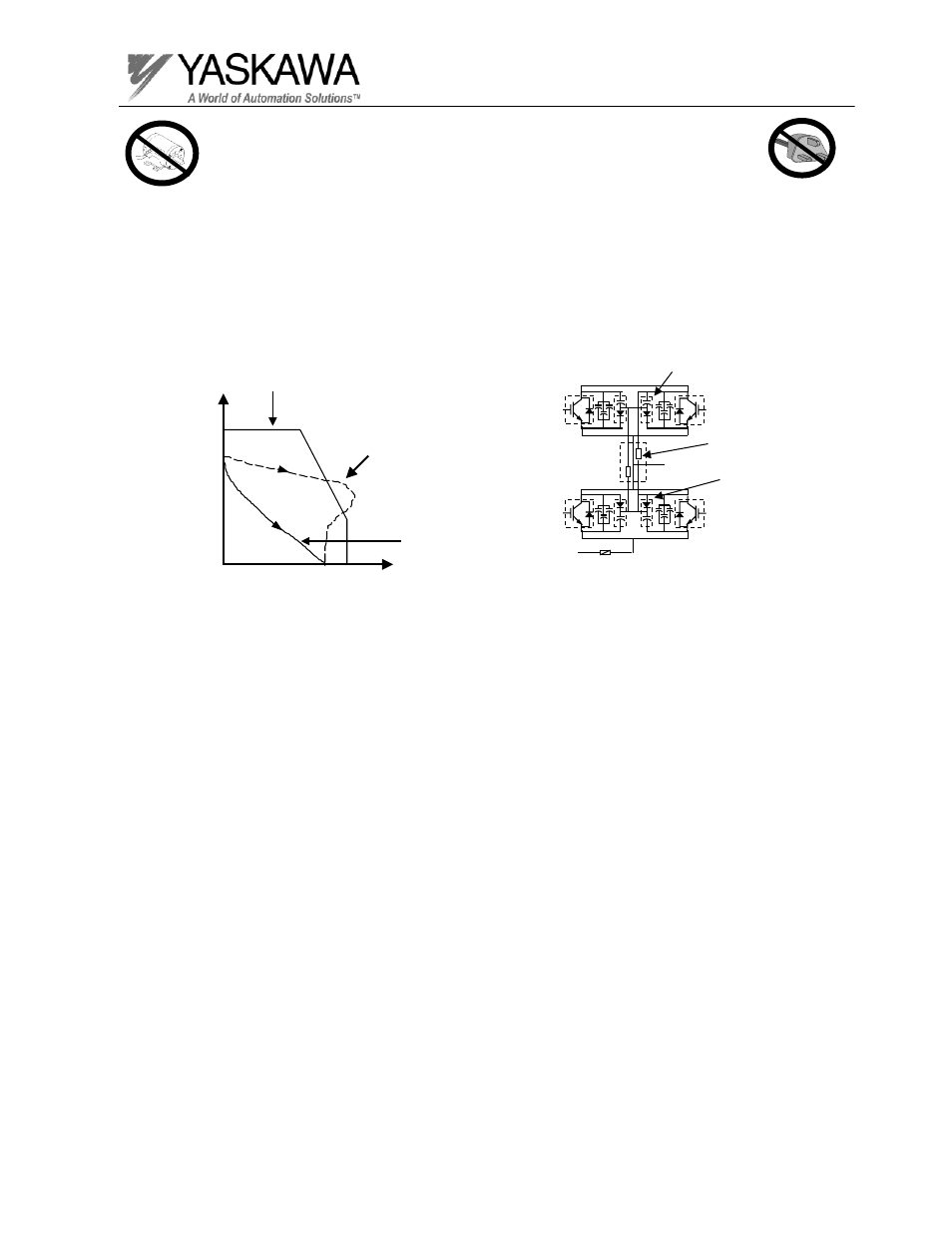
Snubber Circuit
The snubber circuit is located in the main circuit attached to each of the
output transistors between the collector and the emitter. The snubber circuit
is typically found in 18kW models and larger. The snubber circuit may
contain a capacitor, diode, and a resistor. When the IGBT is turned off, it
may be damaged from surge voltage generated by unit wiring inductance.
The snubber circuit absorbs the surge voltage to keep the voltage within the
SOA (safe operating area) of the output transistor.
Collector
Current (Ic)
Voltage between Collector and Emitter (Vc-E)
Without Snubber
With Snubber
Reverse Bias SOA
0
Output transistors
with snubber circuit
Resistors
Capacitors
Diodes
Advertising
This manual is related to the following products: