Communications d - 15 – Yaskawa F7 Drive User Manual User Manual
Page 234
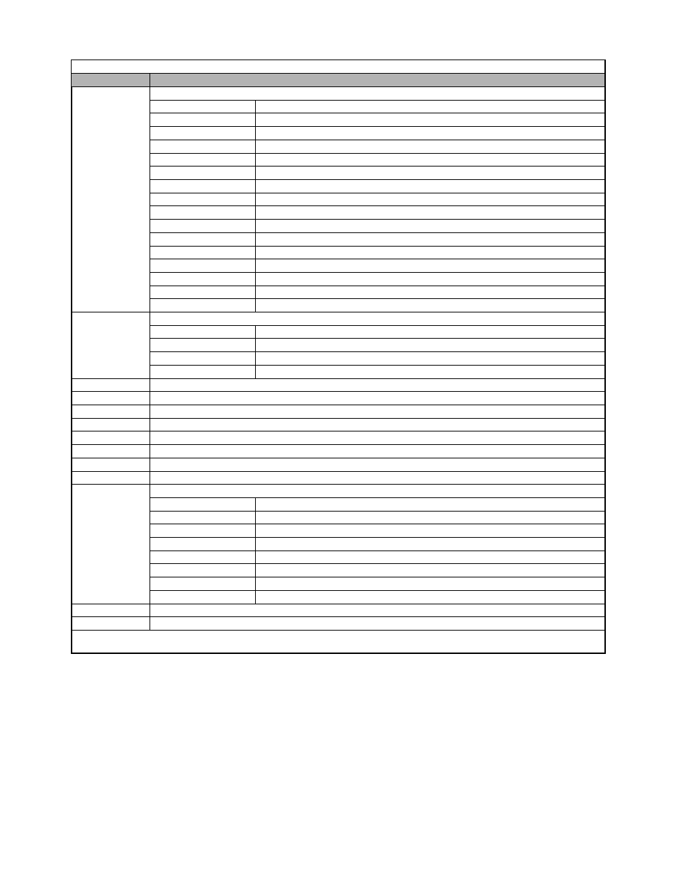
Communications D - 15
002CH
Drive status
Bit 0
Operation:
Operating = 1
Bit 1
Zero speed:
Zero speed = 1
Bit 2
Frequency agree:
Matched = 1
Bit 3
Desired frequency agree:
Matched = 1
Bit 4
Frequency detection 1:
Output frequency
≤ L4-01 = 1
Bit 5
Frequency detection 2:
Output frequency
≥ L4-01 = 1
Bit 6
Drive start-up completed:
Start-up completed = 1
Bit 7
Low voltage detection:
Detected = 1
Bit 8
Baseblock:
Drive output baseblock = 1
Bit 9
Frequency reference mode:
Not communication = 1 Communication = 0
Bit A
Run command mode:
Not communication = 1 Communication = 0
Bit B
Overtorque detection:
Detected = 1
Bit C
Frequency reference lost:
Lost = 1
Bit D
Retrying error:
Retrying = 1
Bit E
Error (including Modbus communications time-out): Error occurred = 1
Bit F
Modbus communications time-out Timed out = 0
002DH
Multi-function digital output status
Bit 0
Multi-function digital output 1 (terminal M1-M2): ON = 1 OFF = 0
Bit 1
Multi-function digital output 2 (terminal M3-M4): ON = 1 OFF = 0
Bit 2
Multi-function digital output 3 (terminal M5-M6): ON = 1 OFF = 0
Bits 3 to F
Not used
002EH - 0030H
Not used
0031H
Main circuit DC voltage
0032H - 0037H
Not used
0038H
PID feedback level (Input equivalent to 100%/Max. output frequency; 10/1%; without sign)
0039H
PID input level (±100%/±Max. output frequency; 10/1%; with sign)
003AH
PID output level (±100%/±Max. output frequency; 10/1%; with sign)
003BH
CPU software number
003CH
Flash software number
003DH
Communication error details
Bit 0
CRC error
Bit 1
Invalid data length
Bit 2
Not used
Bit 3
Parity error
Bit 4
Overrun error
Bit 5
Framing error
Bit 6
Time-out
Bits 7 to F
Not used
003EH
kVA setting
003FH
Control method
Note: Communication error details are stored until an error reset is input (errors can be reset while the Drive is operating).
Note: Write 0 to all unused bits. Do not write data to reserved or “Not Used” registers and bits.
Table D.5 Monitor Data (Continued)
Register No.
Contents