Performing pfl simulation for fpga configuration – Altera Parallel Flash Loader IP User Manual
Page 31
Related Information
•
•
Provides more information about obtaining the .vo or .vho, .sdo, and simulation libraries in the
ModelSim-Altera software.
Performing PFL Simulation for FPGA Configuration
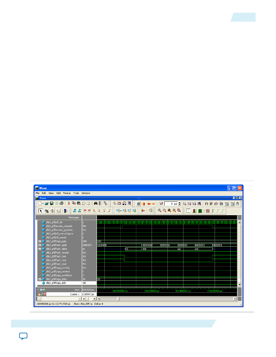
Before beginning the FPGA configuration, the PFL IP core reads the option bits stored in the option bits
sector to obtain information about the
.pof
version used for flash programming, the start and end address
of each page of the configuration image stored in the flash, and the Page-Valid bit.
In this simulation example, the start and end addresses of the option bits sector are
0×800000
and
0×800080
, respectively. The PFL IP core first reads from the final address, which is
0×800080
, to obtain
the
.pof
version information. Because
fpga_pgm[2..0]
is set to 000, the PFL IP core reads from address
0×800000
to address
0×800003
to get the start and end address of page 0 and the Page-Valid bit. The LSB
in address
0×800000
is the Page-Valid bit.
The Page-Valid bit must be 0 for the PFL IP core to proceed with FPGA configuration. While the PFL IP
core reads from the flash, it asserts the active-low
flash_nce
and
flash_noe
signals, and asserts the
active-high
pfl_flash_access_request
signal.
Note: Before you perform the device configuration simulation, ensure that the PFL IP core receives the
correct option bits address and associated values to guarantee correct simulation output.
Figure 21: Simulation Before Configuration
Figure shows the simulation when the PFL IP core reads the option bits from the flash memory device
before configuration starts.
UG-01082
2015.01.23
Performing PFL Simulation for FPGA Configuration
31
Parallel Flash Loader IP Core User Guide
Altera Corporation