Functional description, Programming flash memory, Programming cfi flash – Altera Parallel Flash Loader IP User Manual
Page 9
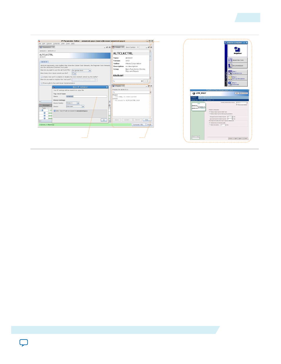
Figure 3: IP Parameter Editors
View IP port
and parameter
details
Apply preset parameters for
specific applications
Specify your IP variation name
and target device
Legacy parameter
editors
Functional Description
The PFL IP core allows you to program flash memory devices with Altera CPLDs through the JTAG
interface and provides the logic to control configuration from the flash memory device to the Altera
FPGA.
Programming Flash Memory
You can use the PFL IP core to program the following flash memory devices with JTAG interface:
• Programming CFI Flash
• Programming Quad SPI Flash
• Programming NAND Flash
Related Information
•
Supported Flash Memory Devices
on page 2
•
Third-party Programmer Support
on page 39
Provides more information about programming the flash memory using third-party tools.
Programming CFI Flash
Altera configuration devices support programming through the JTAG interface to allow in-system
programming and updates. However, standard flash memory devices do not support the JTAG interface.
You can use the JTAG interface in Altera CPLDs to indirectly program the flash memory device.
The Altera CPLD JTAG block interfaces directly with the logic array in a special JTAG mode. This mode
brings the JTAG chain through the logic array instead of the Altera CPLD boundary-scan cells (BSCs).
UG-01082
2015.01.23
Functional Description
9
Parallel Flash Loader IP Core User Guide
Altera Corporation