Signals – Altera Parallel Flash Loader IP User Manual
Page 44
Signals
This section contains information about the PFL IP core input and output signals.
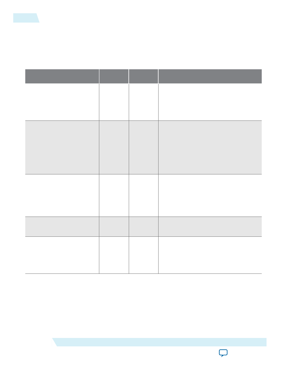
Table 14: PFL Signals
For maximum FPGA configuration
DCLK
frequencies, refer to the Configuration Handbook.
Pin
Description
Weak Pull-
Up
Function
pfl_nreset
Input
—
Asynchronous reset for the PFL IP core. Pull
high to enable FPGA configuration. To
prevent FPGA configuration, pull low when
you do not use the PFL IP core. This pin
does not affect the flash programming
functionality of the PFL IP core.
pfl_flash_access_granted
Input
—
Used for system-level synchronization. This
pin is driven by a processor or any arbitrator
that controls access to the flash. This active-
high pin is connected permanently high if
you want the PFL IP core to function as the
flash master. Pulling the
pfl_flash_
access_granted
pin low prevents the JTAG
interface from accessing the flash and FPGA
configuration.
pfl_clk
Input
—
User input clock for the device. Frequency
must match the frequency specified in the IP
core and must not be higher than the
maximum
DCLK
frequency specified for the
specific FPGA during configuration. This
pins are not available for the flash program‐
ming option in the PFL IP core.
fpga_pgm[]
Input
—
Determines the page for the configuration.
This pins are not available for the flash
programming option in the PFL IP core.
fpga_conf_done
Input
10-kW Pull-
Up Resistor
Connects to the
CONF_DONE
pin of the FPGA.
The FPGA releases the pin high if the
configuration is successful. During FPGA
configuration, this pin remains low. This
pins are not available for the flash program‐
ming option in the PFL IP core.
44
Signals
UG-01082
2015.01.23
Altera Corporation
Parallel Flash Loader IP Core User Guide