Factory default switch settings, Factory default switch settings –2, Figure 4–1 – Altera Stratix IV E FPGA User Manual
Page 18: Shows the
Advertising
4–2
Chapter 4: Development Board Setup
Factory Default Switch Settings
Stratix IV E FPGA Development Kit User Guide
June 2011
Altera Corporation
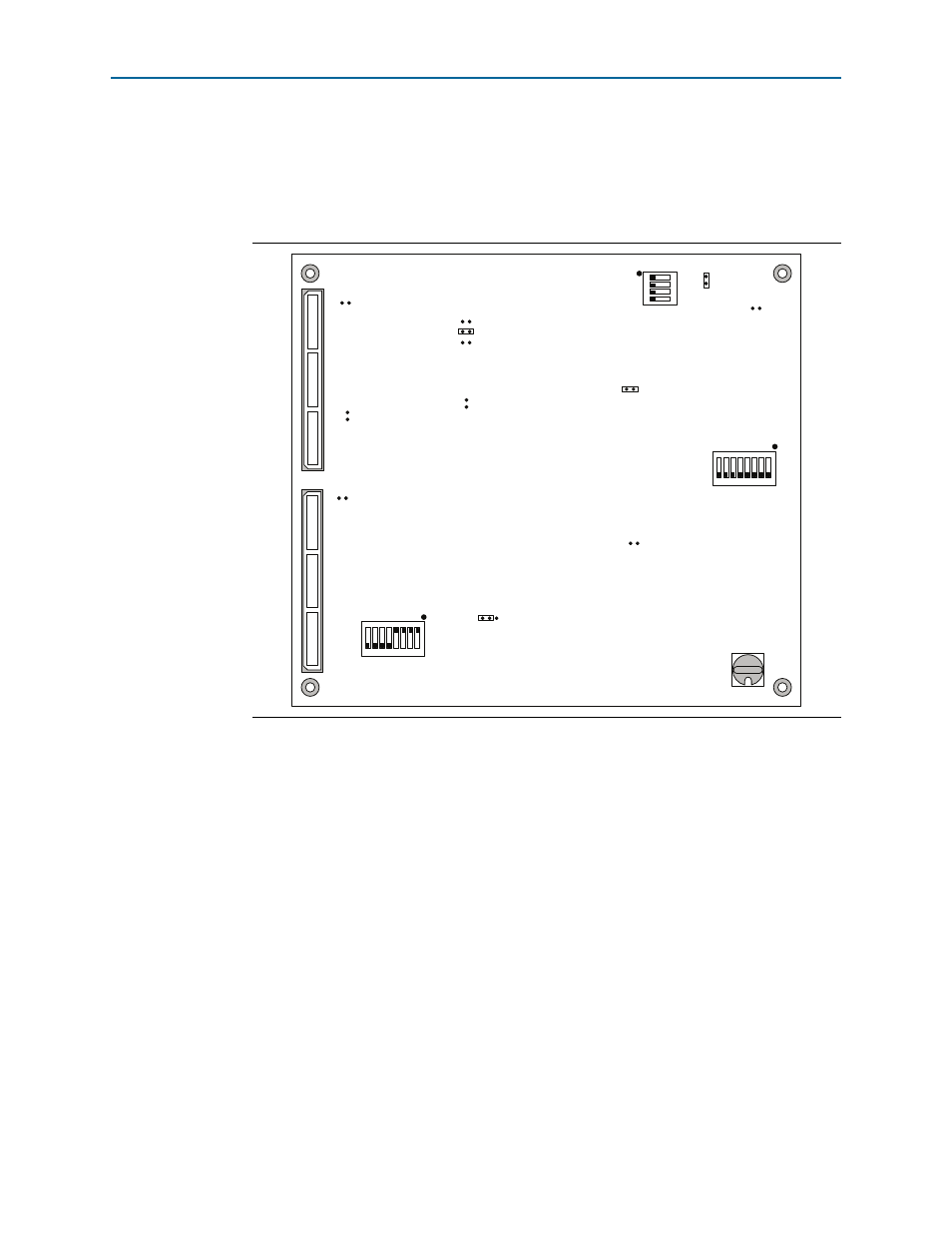
Factory Default Switch Settings
This section shows the factory switch settings for the Stratix IV E FPGA development
board.
shows the switch locations and the default position of each switch
on the top side of the board.
Figure 4–1. Switch Locations and Default Settings on the Board Top
1
2
3
4
5
6
7
8
ON
4
3
2
1
1
2
3
4
5
6
7
8
0
1 2 3
QDRII_DRIVE
60
50
MIN
J7
VCC_VCCL_SEL
J21
USB
J4
Clock
Enable
SW1
MSEL0
J2
MAXII_JTAG_EN
J10
SHUNT = 1.8V_QDR
J11
FAN
J12
HSMB JTAG EN
J5
HSMA_JTAG_EN
J15
SHUNT = 1.8V_RLD
J18
SW5
SW2
MAX II DIPSWITCH
Rotary
Switch
OPEN
OPEN
SW4
Board Settings
PGM CONFIG SELECT
Advertising