The ssram tab, The ssram tab –11, Read –11 – Altera Stratix IV E FPGA User Manual
Page 37: Read
Chapter 6: Board Test System
6–11
Using the Board Test System
June 2011
Altera Corporation
Stratix IV E FPGA Development Kit User Guide
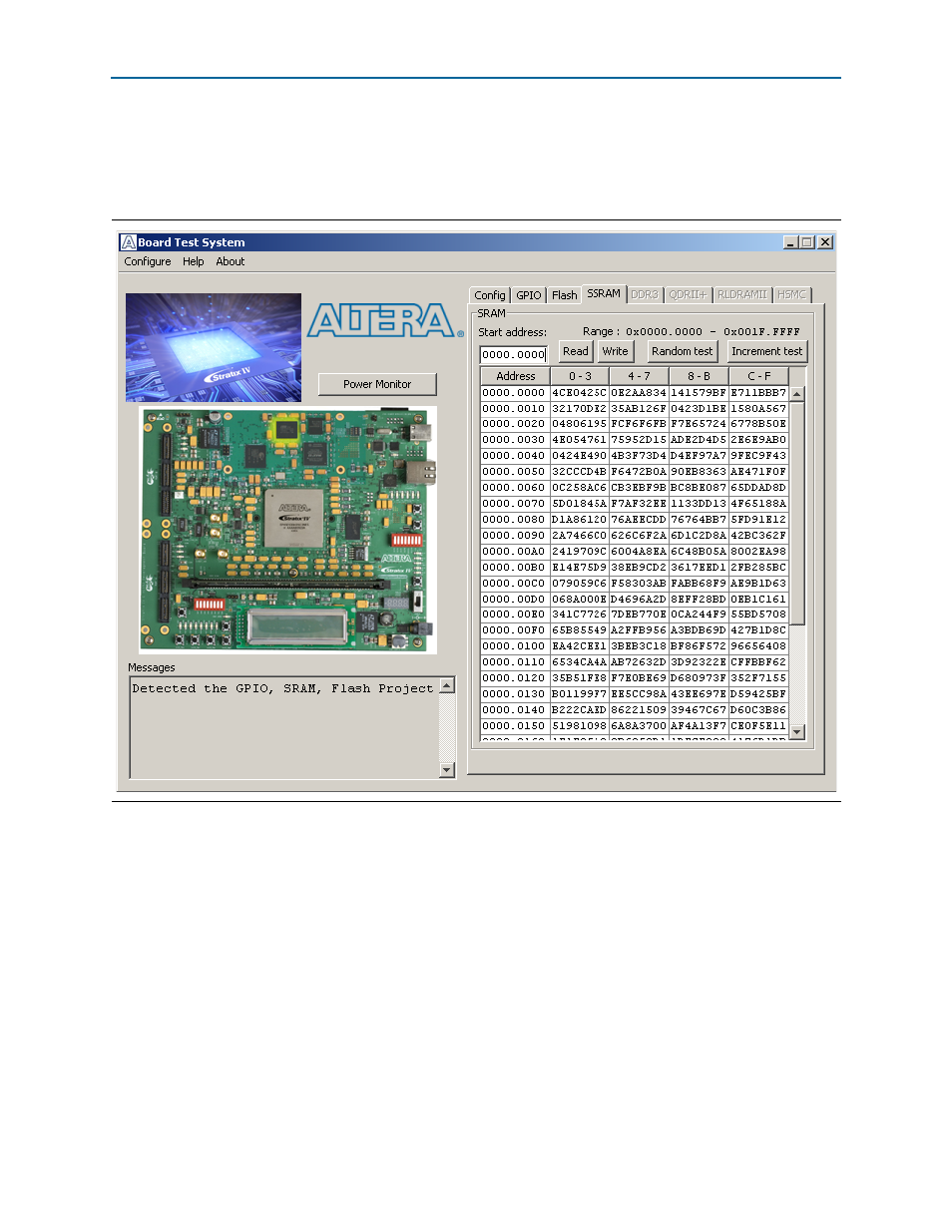
The SSRAM Tab
The SSRAM tab allows you to read and write SSRAM on your board.
Figure 6–5
shows the SSRAM tab.
The following sections describe the controls on the SSRAM tab.
Read
Reads the SSRAM on your board. To see the SSRAM contents, type a starting address
in the text box and click Read. Values starting at the specified address appear in the
table. The base address of SRAM in this Nios II-based BTS design is 0x0D00.0000. The
valid address range within the 2-MB SRAM is 0x0000.0000 through 0x001F.FFFF, as
shown in the GUI.
1
If you enter an address outside of the 0x0000.0000 to 0x001F.FFFF SSRAM address
space, a warning message identifies the valid SSRAM address range.
Figure 6–5. The SSRAM Tab