Altera Stratix IV GX FPGA Development Board User Manual
Page 11
Chapter 2: Board Components
2–3
Board Overview
November 2010
Altera Corporation
Stratix IV GX FPGA Development Board, 530 Edition Reference Manual
D26
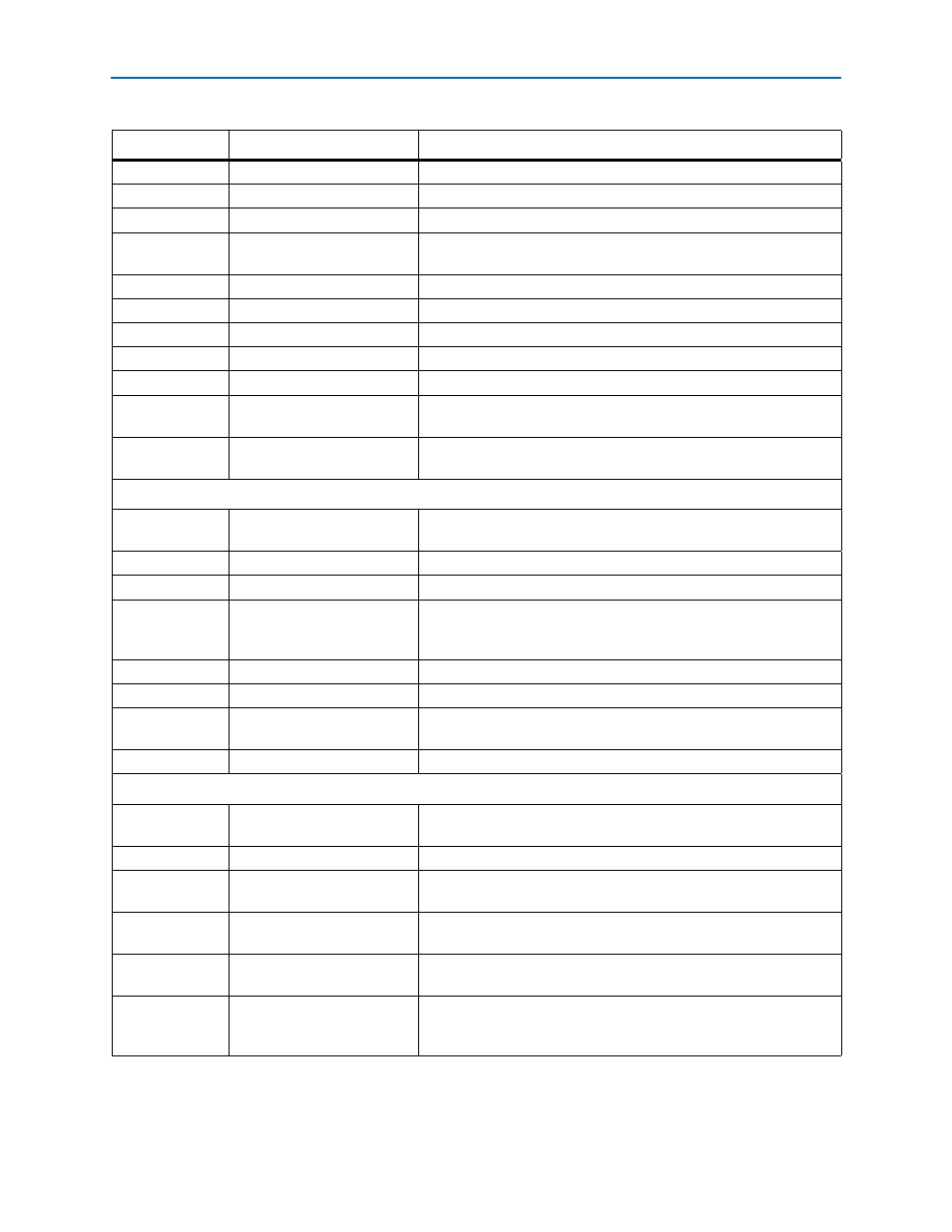
Load LED
Illuminates during embedded USB-Blaster data transfers.
D27
Error LED
Illuminates when the FPGA configuration from flash fails.
D24
Power LED
Illuminates when 12-V power is present.
D32, D33, D34,
D35
Ethernet LEDs
Shows the connection speed as well as transmit or receive activity.
D3, D4
HSMC port A LEDs
You can configure these LEDs to indicate transmit or receive activity.
D1
HSMC port A Present LED
Illuminates when a daughtercard is plugged into the HSMC port A.
D14, D15
HSMC port B LEDs
You can configure these LEDs to indicate transmit or receive activity.
D2
HSMC port B Present LED
Illuminates when a daughtercard is plugged into the HSMC port B.
D30
SDI mute LED
Illuminates when the SDI receiver is muted.
D25
PCI Express Gen 2 LED
You can configure this LED to illuminate when PCI Express is in Gen 2
mode.
D37, D38, D39
PCI Express Link LEDs
You can configure these LEDs to display the PCI Express link width
(x1, x4, x8).
Clock Circuitry
X1
125 M oscillator
125.000-MHz crystal oscillator for Gigabit Ethernet, Serial RapidIO™
(SRIO), or PCI Express.
X2
156 M oscillator
156.250-MHz crystal oscillator for 10 Gigabit Ethernet or XAUI.
X3
148 M oscillator
148.500-MHz voltage controlled crystal oscillator for SDI Video.
X6
100 M oscillator
100.000-MHz (programmable to any frequency between 20–810 MHz)
crystal oscillator for PCI Express or general use such as memories.
Multiplex with CLKIN_SMA_P based on CLK_SEL switch value.
X7
155 M oscillator
155.520-MHz crystal oscillator for SONET.
X8
50 M oscillator
50.000-MHz crystal oscillator for general purpose logic.
J15, J14
Clock input SMAs
Drives LVPECL-compatible clock inputs into the U50 clock multiplexer
buffer.
J9
Clock output SMA
Drives out 2.5-V CMOS clock outputs from the FPGA.
General User Input and Output
D6-D13
D16-D23
User LEDs
16 user LEDs. Illuminates when driven low.
SW3
User DIP switch
Octal user DIP switches. When the switch is ON, a logic 0 is selected.
S1
Reset configuration
push-button switch
Press to reconfigure the FPGA from the flash memory.
S2
CPU reset push-button switch
Press to reset the Max II CPLD EPM2210 System Controller and FPGA
logic.
S3, S4, S5
General user push-button
switches
Three user push-button switches. Driven low when pressed.
SW2
Power monitor rotary switch
Selects the power rail being measured. It also selects the FPGA image
to load on power-up; 0 selects factory image and 1 selects
user-defined image.
Table 2–1. Stratix IV GX FPGA Development Board, 530 Edition Components (Part 2 of 3)
Board Reference
Type
Description