Altera Stratix IV GX FPGA Development Board User Manual
Page 57
Chapter 2: Board Components
2–49
Memory
November 2010
Altera Corporation
Stratix IV GX FPGA Development Board, 530 Edition Reference Manual
U5, U12, U18, U24 pin P3
Address bus
DDR3BOT_A2
1.5-V SSTL Class I
AH14
U5, U12, U18, U24 pin P7
Address bus
DDR3BOT_A1
AG15
U5, U12, U18, U24 pin N3
Address bus
DDR3BOT_A0
AK13
U5, U12, U18, U24 pin M3
Bank address bus
DDR3BOT_BA2
AE15
U5, U12, U18, U24 pin M3
Bank address bus
DDR3BOT_BA1
AD15
U5, U12, U18, U24 pin M3
Bank address bus
DDR3BOT_BA0
AF14
U5, U12, U18, U24 pin J3
Row address select
DDR3BOT_RASn
AW21
U5, U12, U18, U24 pin K3
Column address select
DDR3BOT_CASn
AV19
U5, U12, U18, U24 pin L2
Chip select
DDR3BOT_CSn
AN20
U5, U12, U18, U24 pin L3
Write enable
DDR3BOT_WEn
AW20
U5, U12, U18, U24 pin K1
Termination enable
DDR3BOT_ODT
AU20
U5, U12, U18, U24 pin K9
Clock enable
DDR3BOT_CKE
AW19
U5, U12, U18, U24 pin J7
Clock P
DDR3BOT_CK_P
AE20
U5, U12, U18, U24 pin K7
Clock N
DDR3BOT_CK_N
AF20
U5.E3
Data bus byte lane 0
DDR3BOT_DQ0
AM14
U5.F7
Data bus byte lane 0
DDR3BOT_DQ1
AM13
U5.F2
Data bus byte lane 0
DDR3BOT_DQ2
AN14
U5.F8
Data bus byte lane 0
DDR3BOT_DQ3
AL14
U5.H3
Data bus byte lane 0
DDR3BOT_DQ4
AR14
U5.H8
Data bus byte lane 0
DDR3BOT_DQ5
AN13
U5.G2
Data bus byte lane 0
DDR3BOT_DQ6
AP14
U5.H7
Data bus byte lane 0
DDR3BOT_DQ7
AP13
U5.E7
Write mask byte lane 0
DDR3BOT_DM0
AL13
U5.F3
Data strobe P byte lane 0
DDR3BOT_DQS_P0
AR13
U5.G3
Data strobe N byte lane 0
DDR3BOT_DQS_N0
AT13
U5.D7
Data bus byte lane 1
DDR3BOT_DQ8
AT12
U5.C3
Data bus byte lane 1
DDR3BOT_DQ9
AW14
U5.C8
Data bus byte lane 1
DDR3BOT_DQ10
AU12
U5.C2
Data bus byte lane 1
DDR3BOT_DQ11
AV14
U5.A7
Data bus byte lane 1
DDR3BOT_DQ12
AW11
U5.A2
Data bus byte lane 1
DDR3BOT_DQ13
AU14
U5.B8
Data bus byte lane 1
DDR3BOT_DQ14
AV11
U5.A3
Data bus byte lane 1
DDR3BOT_DQ15
AW12
U5.D3
Write mask byte lane 1
DDR3BOT_DM1
AU11
U5.C7
Data strobe P byte lane 1
DDR3BOT_DQS_P1
AV13
U5.B7
Data strobe N byte lane 1
DDR3BOT_DQS_N1
AW13
U12.E3
Data bus byte lane 2
DDR3BOT_DQ16
AT16
U12.F7
Data bus byte lane 2
DDR3BOT_DQ17
AW16
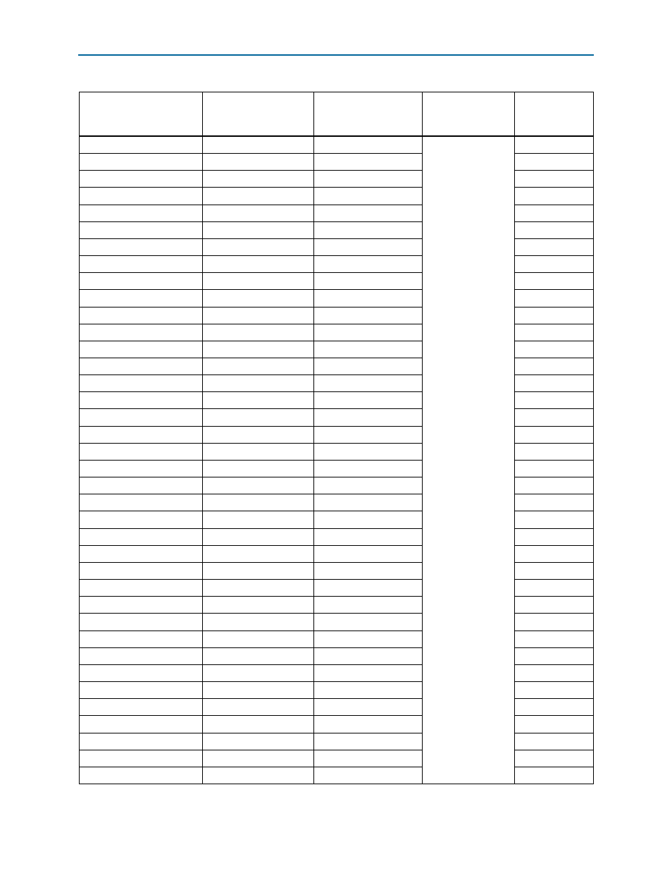
Table 2–46. DDR3 Bottom Port Pin Assignments, Schematic Signal Names, and Functions (Part 2 of 4)
Board Reference
Description
Schematic Signal
Name
I/O Standard
Stratix IV GX
Device
Pin Number