User-defined dip switches, User-defined dip switches –27 – Altera Stratix IV GX FPGA Development Board User Manual
Page 35
Chapter 2: Board Components
2–27
General User Input/Output
November 2010
Altera Corporation
Stratix IV GX FPGA Development Board, 530 Edition Reference Manual
Board reference S2 is the CPU reset push-button switch, CPU_RESETn, which is an input
to both the Stratix IV GX device and MAX
II CPLD EPM2210 System Controller. The
CPU_RESETn
is intended to be the master reset signal for the FPGA design loaded into
the Stratix IV GX device. The CPU_RESETn signal must be enabled within the Quartus II
software for this reset function to work. Otherwise, the CPU_RESETn acts as a regular
I/O pin. When enabled in the Quartus II software, and then pulled high on the board,
this switch resets every register within the FPGA.
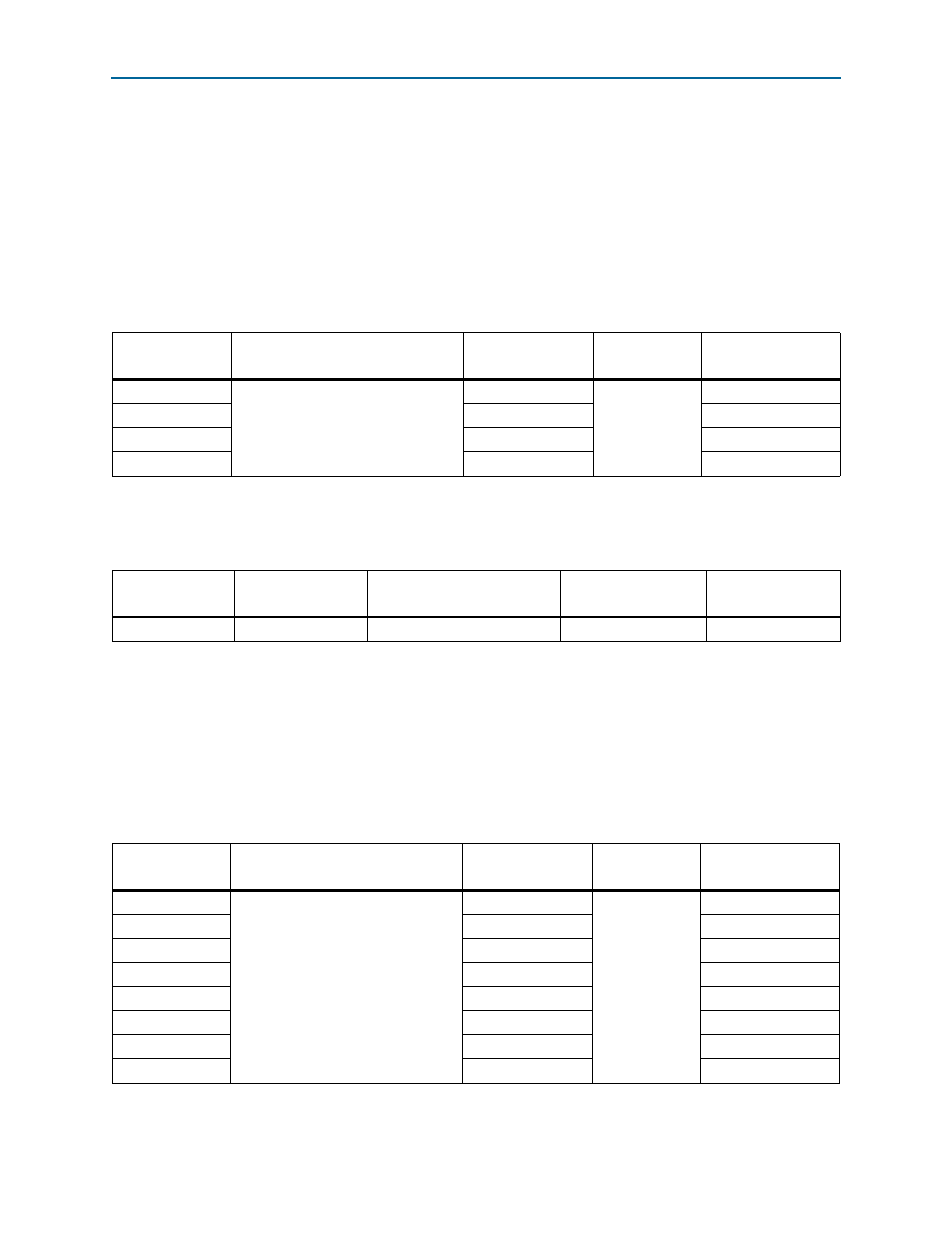
Table 2–23
lists the user-defined push-button switch schematic signal names and their
corresponding Stratix IV GX device pin numbers.
lists the user-defined push-button switch component reference and the
manufacturing information.
User-Defined DIP Switches
Board reference S6 is an 8-pin DIP switch. The switches in S6 are user-defined, and are
provided for additional FPGA input control. There is no board-specific function for
these switches.
Table 2–25
lists the user-defined DIP switch schematic signal names and their
corresponding Stratix IV GX pin numbers.
Table 2–23. User-Defined Push-Button Switch Schematic Signal Names and Functions
Board Reference
Description
Schematic Signal
Name
I/O Standard
Stratix IV GX Device
Pin Number
S2
User-Defined push-button switch
CPU_RESETn
2.5-V
V34
S3
USER_PB2
M34
S4
USER_PB1
W32
S5
USER_PB0
AK35
Table 2–24. User-Defined Push-Button Switch Component Reference and Manufacturing Information
Board Reference
Description
Manufacturer
Manufacturer
Part Number
Manufacturer
Website
S2 to S5
Push-Button switch
Panasonic Corporation
EVQPAC07K
Table 2–25. User-Defined DIP Switch Schematic Signal Names and Functions
Board Reference
Description
Schematic
Signal Name
I/O Standard
Stratix IV GX Device
Pin Number
SW3.1
User-Defined DIP switch connected to
FPGA device. When the switch is in
the OPEN or OFF position, a logic 1 is
selected. When the switch is in the
CLOSED or ON position, a logic 0 is
selected.
USER_DIPSW0
2.5-V
AL35
SW3.2
USER_DIPSW1
AC35
SW3.3
USER_DIPSW2
J34
SW3.4
USER_DIPSW3
AN35
SW3.5
USER_DIPSW4
G33
SW3.6
USER_DIPSW5
K35
SW3.7
USER_DIPSW6
AG34
SW3.8
USER_DIPSW7
AG31