Development board block diagram, Handling the board – Altera Stratix IV GX FPGA Development Board User Manual
Page 8
1–4
Chapter 1: Overview
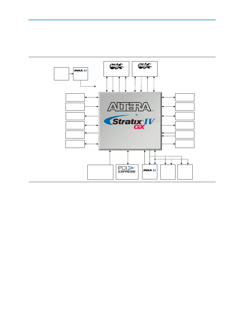
Development Board Block Diagram
Stratix IV GX FPGA Development Board, 530 Edition Reference Manual
November 2010
Altera Corporation
Development Board Block Diagram
shows the block diagram of the Stratix IV GX FPGA Development Board,
530 Edition.
Handling the Board
When handling the board, it is important to observe the following static discharge
precaution:
c
Without proper anti-static handling, the board can be damaged. Therefore, use
anti-static handling precautions when touching the board.
Figure 1–1. Stratix IV GX FPGA Development Board, 530 Edition Block Diagram
EP4SGX530KH40
Port A
Port B
128 Mbytes
DDR3 TOP
4 Mbytes
QDRII+ TOP 0
4 Mbytes
QDRII+ TOP 1
XCVR
SMA OUT
Buttons
Switches
LED
CPLD
64 Mbytes
FLASH
2 Mbytes
SSRAM
x8 Edge
Oscillators
50 MHz, 100 MHz,
125 MHz, 148 MHz,
155 MHz, 156 MHz
512 Mbytes
DDR3 BOT
REFCLK
SMA IN
TRIG
SMA OUT
GigE
PHY
HDMI
TX
SDI
TX/TX
Embedded
Blaster
USB
2.0
x64
x1 (LVPECL)
x1
x1
x24
XCVR x1
x16
x16
x16
XCVR x1
x5
x8
x16
x4
XCVR x8
x8 Config
x32
x80
CLKIN x3
CLKOUT x3
XCVR x8
x80
CLKIN x3
CLKOUT x3
XCVR x6
ADDR
JTAG Chain