Power distribution system, Power distribution system –64, Figure 2–15. power distribution system – Altera Stratix IV GX FPGA Development Board User Manual
Page 72
2–64
Chapter 2: Board Components
Power Supply
Stratix IV GX FPGA Development Board, 530 Edition Reference Manual
November 2010
Altera Corporation
Power Distribution System
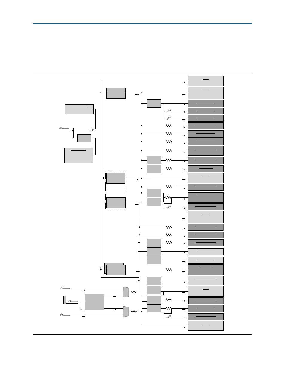
Figure 2–15
shows the power distribution system on the development board.
Regulator inefficiencies and sharing are reflected in the currents shown, which are
conservative absolute maximum levels.
Figure 2–15. Power Distribution System
Switching
Regulator
LTM4614
Dual-Switching
Regulator
0.9 V
12.803 A
12V
HSMC Port A and B
FPGA Cooling Fan
S4VCC
S4 Core VCC
S4 VCCHIP
12 V
2.095 A
2x LTM4601
Switching
Regulator
2.5 V
0.837 A
LTM4601
Switching
Regulator
1.8V
QDRII VDD, Flash VDD,
EPM2210 VCCINT
1.8 V
1.971 A
LT3080
Linear
S4VCCH_GXB
S4 Transceiver VCCH_GXB
1.4 V
0.567 A
LT3080-1
Linear
LT3080-1
Linear
1.1 V
1.343 A
LT3025-1
Linear
S4VCCPT
S4 VCCPT
1.5 V
0.286 A
2.5 V
10.13 A
1.8 V
3.417 A
1.5V
DDR3 VDD/VDDQ,
QDRII VDDQ,
S4 VCCIO B3/B4/B7/B8
1.5 V
2.100 A
1.5 V
3.871 A
LT3025-1
Linear
S4VCCD_PLL
S4 VCCD_PLL
0.9 V
0.100 A
LT3025-1
Linear
ENET_DVDD
Enet PHY DVDD
1.0 V
0.253 A
0.9 V
12.803 A
S4VCCIO_B1B2
S4 Banks 1 & 2 VCCIO
S4VCCIO_B5
S4 Bank 5 VCCIO
S4VCCIO_B6
S4 Bank 6 VCCIO
S4VCCIO_INT
S4 VCC_CLKIN, VCCPGM,
VCCPD
2.5V
Sync SRAM, Flash VDDQ,
NB6L11S, Enet PHY AVDD,
EPM2210, 7 Oscillators
2.5 V
0.484 A
2.5 V
0.181 A
2.5 V
0.181 A
2.5 V
0.050 A
3.3V_PCIe
0.69 A
(4.77 A with full HSMCs)
3.3V
HSMC Port A and B, SDI
ICS 8543 LVDS Clock Buffer
3.3 V
4.050 A
LT3025-1
Linear
S4VCCAUX
S4 VCCAUX
2.5 V
0.250 A
S4VCCA_GXB
S4 Transceiver VCCA
3.0 V
0.331 A
S4VCCIO_B7B8
S4 Bank 7 & 8 VCCIO
S4VCCIO_B3B4
S4 Bank 3 & 4 VCCIO
1.5 V
0.880 A
1.5 V
0.410 A
R220
14 V - 20 V
DC INPUT
5.75 A
4.77 A
LT3010
Linear
2.5V_USB
EPM240 Emb. Blaster,
USB PHY IO,
24M OSC,
AT93C46DN EEPROM
Only need bottom device
for larger 4SGX530 FPGA
S4VCCA_PLL
S4 VCCA_PLL
2.5 V
0.051 A
(5.75 A with full HSMCs)
ideal
di
ode mux
LTM3727
Dual
Switching
Regulator
12V_SENSE_N
3.3V_SENSE_N
ideal
diode mux
12V_PCIe
3.74 A
S4VCCL_GXB
S4 Transceiver VCCL
1.1 V
0.093 A
S4VCC_GXB
S4 Transceiver
VCCR/VCCT
LT3025-1
Linear
HDMI_PVDD
HDMI Analog
1.8 V
0.080 A
HDMI_DVDD
HDMI Digital
1.8 V
0.100 A
HDMI_AVDD
HDMI TMDS Driver
1.8 V
0.080 A
U38
U8
U49
U46
U48
U17
U41
U44
U45
U50
U10
U6
S4VCCIO_B3A
S4 Bank 3A VCCIO
1.8 V
0.010 A
5V_USB
0.039 A
5.0V_USB
USB PHY Analog,
AT93C46DN EEPROM
5.0 V
0.025 A
BEAD
BEAD
BEAD
BEAD
U51 (bottom-side)
U26 (top-side)
Linear
0.75V_VTT
DDR3BOT ADDR/CMD Term
0.75 V
0.128 A
U52
TPS51100
12 V
3.3 V
R155
R144
R69
R171
R174
R223
R105
R104
R158
R64
R70
LTM8021
Switcher
5.0V
Char LCD, HDMI Cable
Linear Reg Inputs
5.0 V
0.006 A
U11
LT3010
Linear
5.0V_MONITOR
2x LT2418 A/D
Linear Reg Inputs
5.0 V
0.044 A
U57
R187
R200
R52
R53
U35
U15
U19
D44
D45
LT3025-1
Linear