Clock circuitry, Clock circuitry –21 – Altera Stratix IV GX FPGA Development Board User Manual
Page 29
Chapter 2: Board Components
2–21
Clock Circuitry
November 2010
Altera Corporation
Stratix IV GX FPGA Development Board, 530 Edition Reference Manual
lists the rotary switch component reference and manufacturing
information.
Clock Circuitry
This section describes the board's clock inputs and outputs.
D
S4VCCIO_B3B4
1.5
VCCIO_B3
Bank 3 I/O power (DDR3BOT)
VCCIO_B4
Bank 4 I/O power (DDR3BOT)
E
S4VCC_GXB
1.1
VCCR
XCVR analog receive
VCCT
XCVR analog transmit
VCCL_GXB
XCVR clock distribution
F
12 V
12
—
All 12 V power
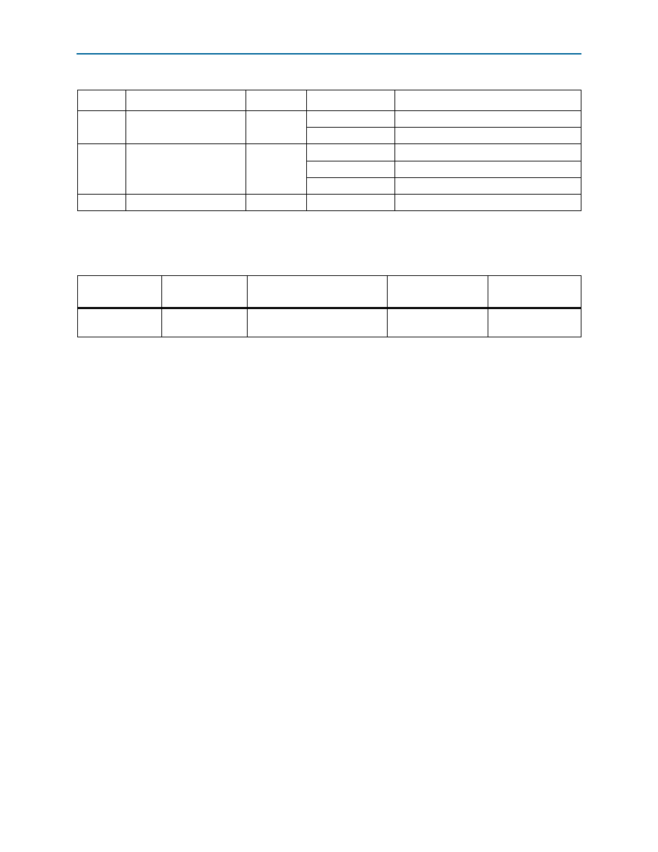
Table 2–18. Power Rail Measurements Based on the Rotary Switch Position (Part 2 of 2)
Switch
Schematic Signal Name
Voltage (V)
Device Pin
Description
Table 2–19. Rotary Switch Component Reference and Manufacturing Information
Board Reference
Description
Manufacturer
Manufacturer
Part Number
Manufacturer
Website
SW2
16-position rotary
switch
Grayhill Corporation
94HCB16WT