Block diagram, Handling the board, Block diagram -4 handling the board -4 – Altera Arria GX Development Board User Manual
Page 10
Advertising
1–4
Reference Manual
Altera Corporation
Arria GX Development Board
October 2007
Handling the Board
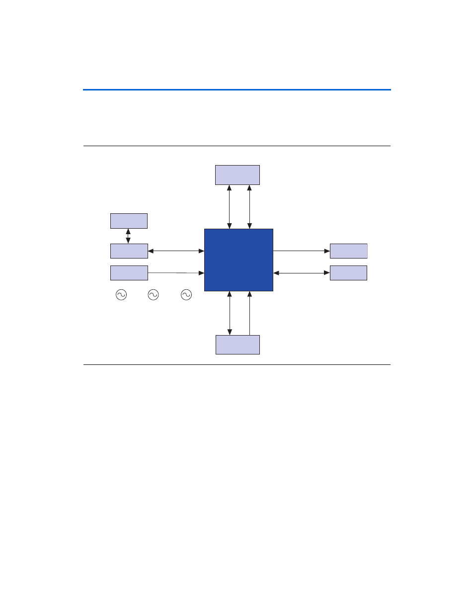
Block Diagram
shows the functional block diagram of the Arria GX
development board.
Figure 1–1. Arria GX Development Board Block Diagram
Handling the
Board
When handling the board it is important to observe the following
precaution:
c
Static Discharge Precaution: Without proper anti-static handling,
the board can be damaged. Therefore, use anti-static handling
precaution when touching the board.
HSMC Port
4x XCVR
CMOS/LVDS
x4 PCIe Edge
Connector
4x XCVR
REFCLK
Arria GX
EP1AGX60DF780
62.5 MHz
100.000 MHz
125 MHz
MAX II
3.3V CMOS
3.3V CMOS
512 MB Flash
Buttons
Switches
TX/RX LEDs
User LEDs
3.3V CMOS
1.8V SSTL
DDR2 SDRAM
MT47H32M16
Advertising