Off-chip memory, Off-chip memory -21 – Altera Arria GX Development Board User Manual
Page 31
Altera Corporation
Reference Manual
2–21
October 2007
Arria GX Development Board
Board Components
Table 2–19
lists the four channel activity LEDs (two per interface).
Off-Chip
Memory
This section describes the board’s DDR2 SDRAM off-chip memory
interface support, providing signal type, and signal connectivity relative
to the Arria GX device.
shows a summary of the required number of pins to support
the 233 MHz DDR2 device available in a 32M x16 data configuration.
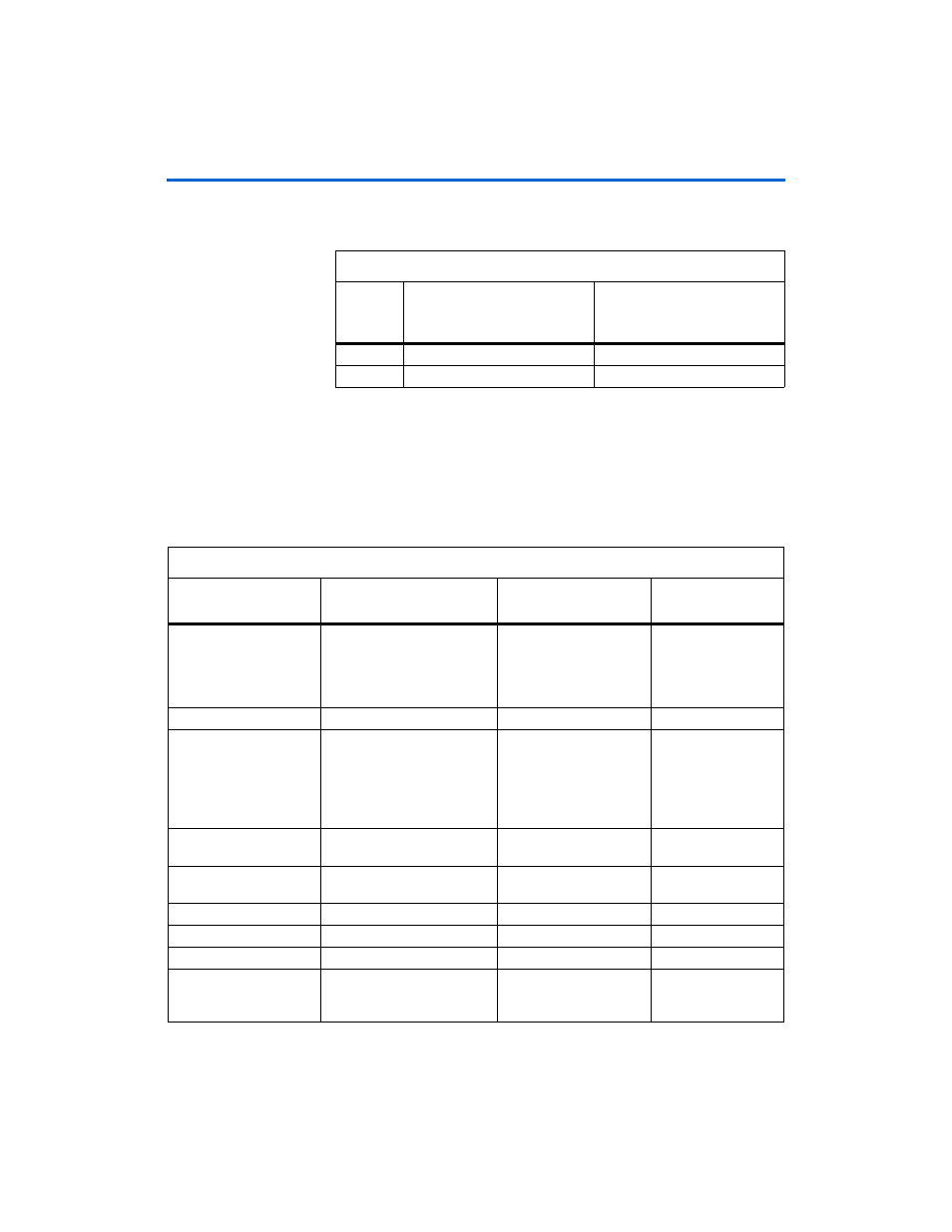
Table 2–19. Channel Activity LEDs
Board
Reference
Number
Transceiver Interface Indicators
Color
D20, D19
PCI edge connector (L0x1, L0x4) Yellow (two per channel)
D13, D12
HSMC (TX & RX)
Yellow (two per channel)
Table 2–20. DDR2 Description, Signal Type, Schematic Signal Name & Arria GX Pin Number (Part 1 of 2)
Description
Signal Type
Schematic Signal Name
Arria GX
Pin Number
Address (row and column) SSTL_18 out (15 bits)
DDR2_A(14:0)
AH9, AF10, AH11,
AG10, AF7, AF13,
AH13, AG8, AH7,
AH12, AH10, AF12,
AF11, AF9, AE7
Bank address
SSTL_18 out (3 bits)
DDR2_BA(1:0)
AF8, AH8
Data
SSTL_18 in/out (16 bits)
DDR2_DQ(15:0)
AF26, AH25, AG26,
AH26, AF22, AH24,
AF24, AH23, AG22,
AH21, AH22, AF21,
AF18, AH20, AF19,
AH18
Data strobe
SSTL_18 DQS in/out
(2 bits)
DDR2_DQS(1:0)
AG23, AH19
Data write mask (byte
enables)
SSTL_18 out (2 bits)
DDR2_DM(1:0)
AF25, AF20
Write enable
SSTL_18 out
DDR2_WEn
AG11
Row address strobe
SSTL_18 out
DDR2_RASn
AH16
Column address strobe
SSTL_18 out
DDR2_CASn
AG16
Differential output clocks
(two DDR loads per p/n
pair)
Diff. SSTL_18 out
(2 bits)
DDR2_CKp(0)
DDR2_CKn(0)
AH15
AH14