Clocking circuitry, Clocking circuitry -15 – Altera Arria GX Development Board User Manual
Page 25
Altera Corporation
Reference Manual
2–15
October 2007
Arria GX Development Board
Board Components
Clocking
Circuitry
Three oscillators of 62.5 MHz, 100 MHz, and 125 MHz are used to clock
the Arria GX transceivers and user logic.
When the board is not plugged into a host, the 100-MHz oscillator is used
to support the transceiver reference clock for PCIe applications.
Figure 2–6
shows the oscillator driving through a four-output LVDS
buffer to a variety of loads. The buffer can either be driven from the
100-MHz oscillator or from the SMA clock input for custom frequencies
or “frequency sweeping” of F
MAX
performance.
1
The CLK_SEL0 pin on the board configuration DIP switch
controls what clock feeds the buffer. See
.
The 62.5 MHz and 125 MHz oscillators ensure that all protocols
supported by the Arria GX device are provided for.
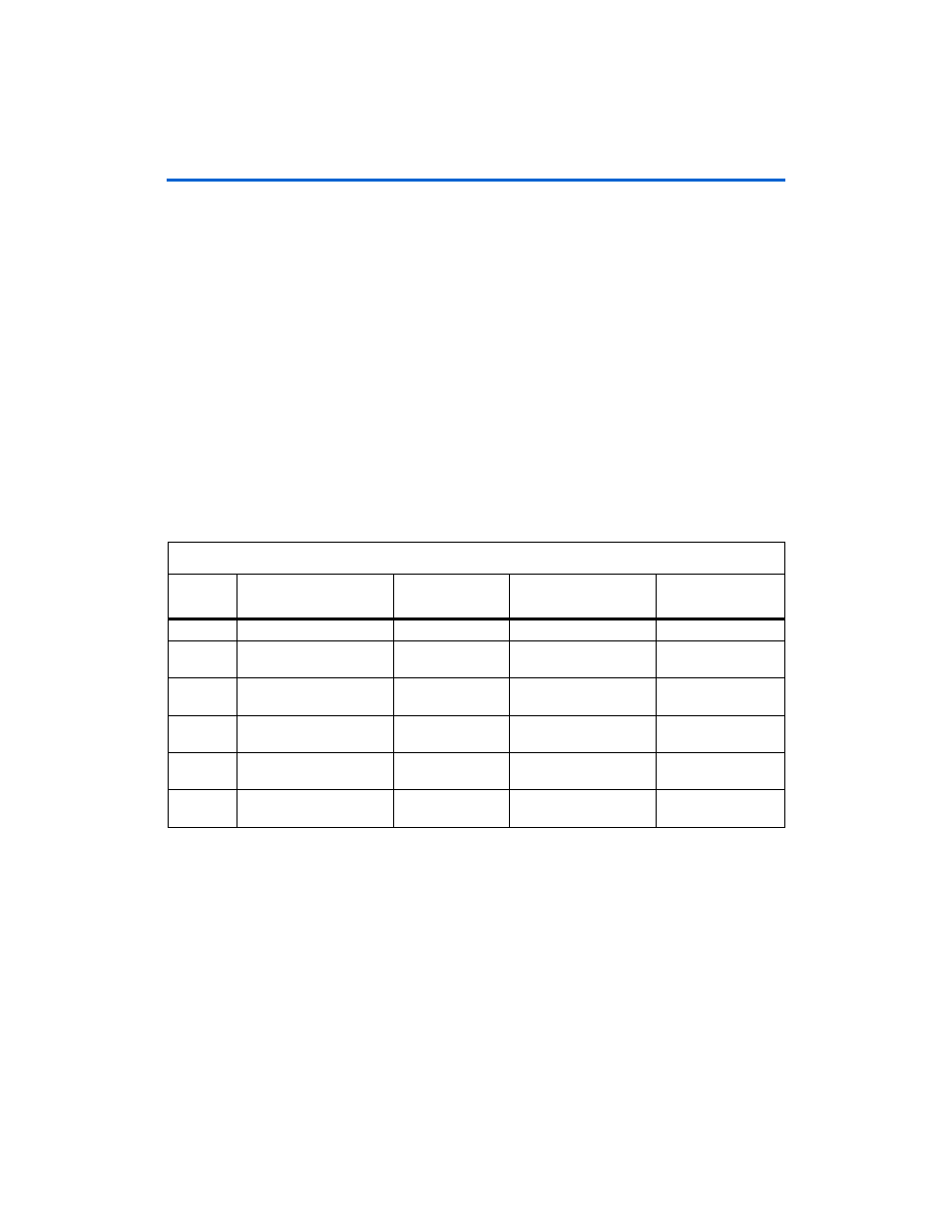
Table 2–11
lists the Arria GX development board’s clocking parts list.
Figure 2–6
shows the oscillator clocking diagram.
Table 2–11. Arria GX Development Board’s Clocking Parts List
Board
Reference
Description
Manufacturer
Manufacturer
Part Number
Manufacturer
Web Site
X3
62.5 MHz LVDS oscillator
Pletronics
LV7745DEV-62.50M
www.pletronics.com
X2
125.00 MHz LVDS
oscillator
Pletronics
LV7745DEV-125.000M
www.pletronics.com
X1
100.00 MHz LVDS
oscillator
Pletronics
LV7745DEV-100.000M
www.pletronics.com
J4
SMA for external clock
input
Lighthorse
Technologies Inc.
LTI-SASF546-P26-X1
www.rfconnector.com
U2
1-to-4 differential-to-LVDS
clock buffer
IDT
ICS8543
www.idt.com
U4
1-to-2 differential-to-single
ended clock buffer
IDT
ICS83026
www.idt.com