Altera Arria GX Development Board User Manual
Page 32
2–22
Reference Manual
Altera Corporation
Arria GX Development Board
October 2007
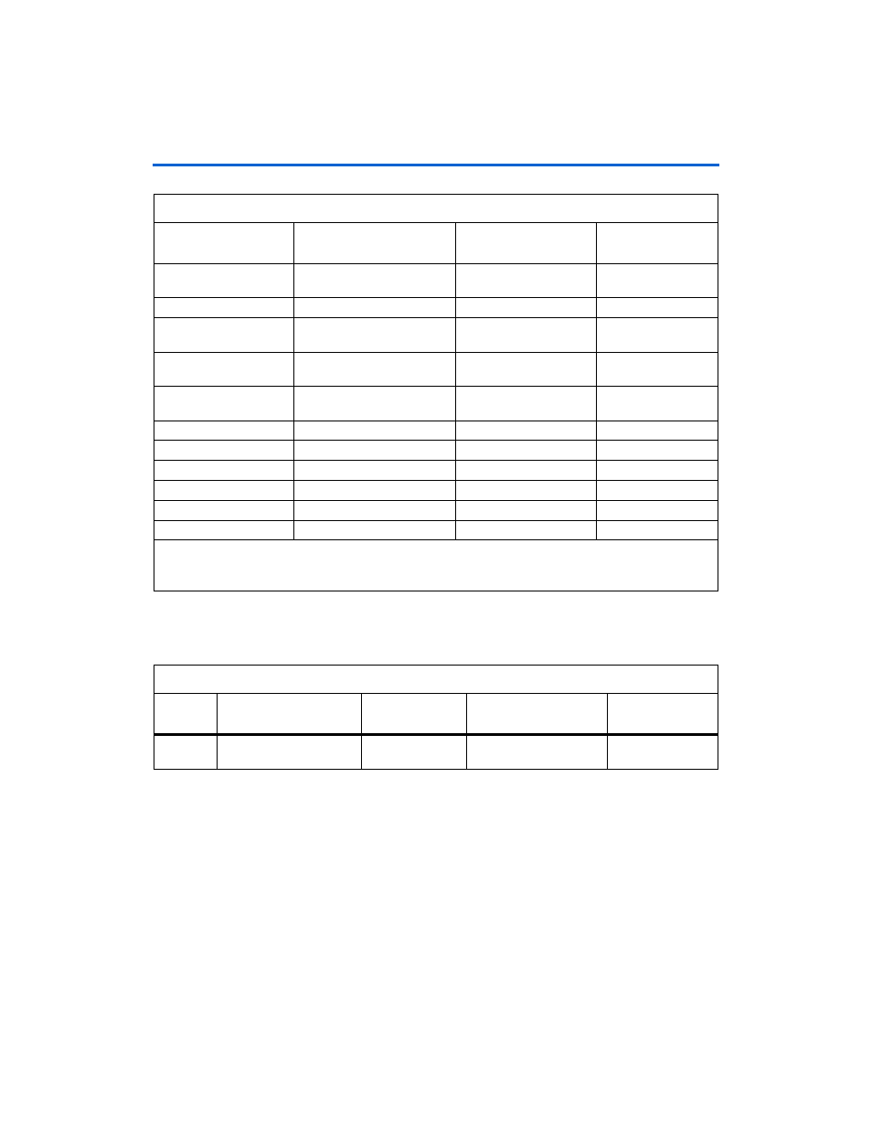
Off-Chip Memory
lists the DDR2 component reference and manufacturing
information.
Resynchronization timing
feedback clock
SSTL_18 out
SSTL_18 in
DDR2_SYNC_CLKOUT
DDR2_SYNC_CLKIN
AG14
AH17
Clock enable
SSTL_18 out
DDR2_CKE
AE14
Chip select (enables
command decoder)
SSTL_18 out
DDR2_CSn
AG13
On-die termination control
pin
SSTL_18 out
DDR2_ODT
AE11
SSTL reference voltage
N/A
Vref
AB14, AC10, AD17,
AD19, AD22, AD8
Core supply
1.8 V
VDD
N/A
(1)
I/O supply
1.8 V
VDDQ
N/A
(1)
DLL supply
1.8 V
VDDL
N/A
(1)
Core GND
Ground
VSS
N/A
(1)
I/O GND
Ground
VSSQ
N/A
(1)
DLL GND
Ground
VSSL
N/A
(1)
Notes to
(1)
This is a power pin that is not connected to the Arria GX device. For power connection information, refer to the
Micron MTA47H32M16 8 Meg X 16 x 4 DDR2 data sheet.
Table 2–20. DDR2 Description, Signal Type, Schematic Signal Name & Arria GX Pin Number (Part 2 of 2)
Description
Signal Type
Schematic Signal Name
Arria GX
Pin Number
Table 2–21. DDR2 Component Reference and Manufacturing Information
Board
Reference
Description
Manufacturer
Manufacturer Part
Number
Manufacturer
Website
U8
DDR2 SDRAM
Micron
Technology, Inc.
MT47H32M16
www.micron.com