Altera Arria GX Development Board User Manual
Page 22
2–12
Reference Manual
Altera Corporation
Arria GX Development Board
October 2007
Configuration Schemes
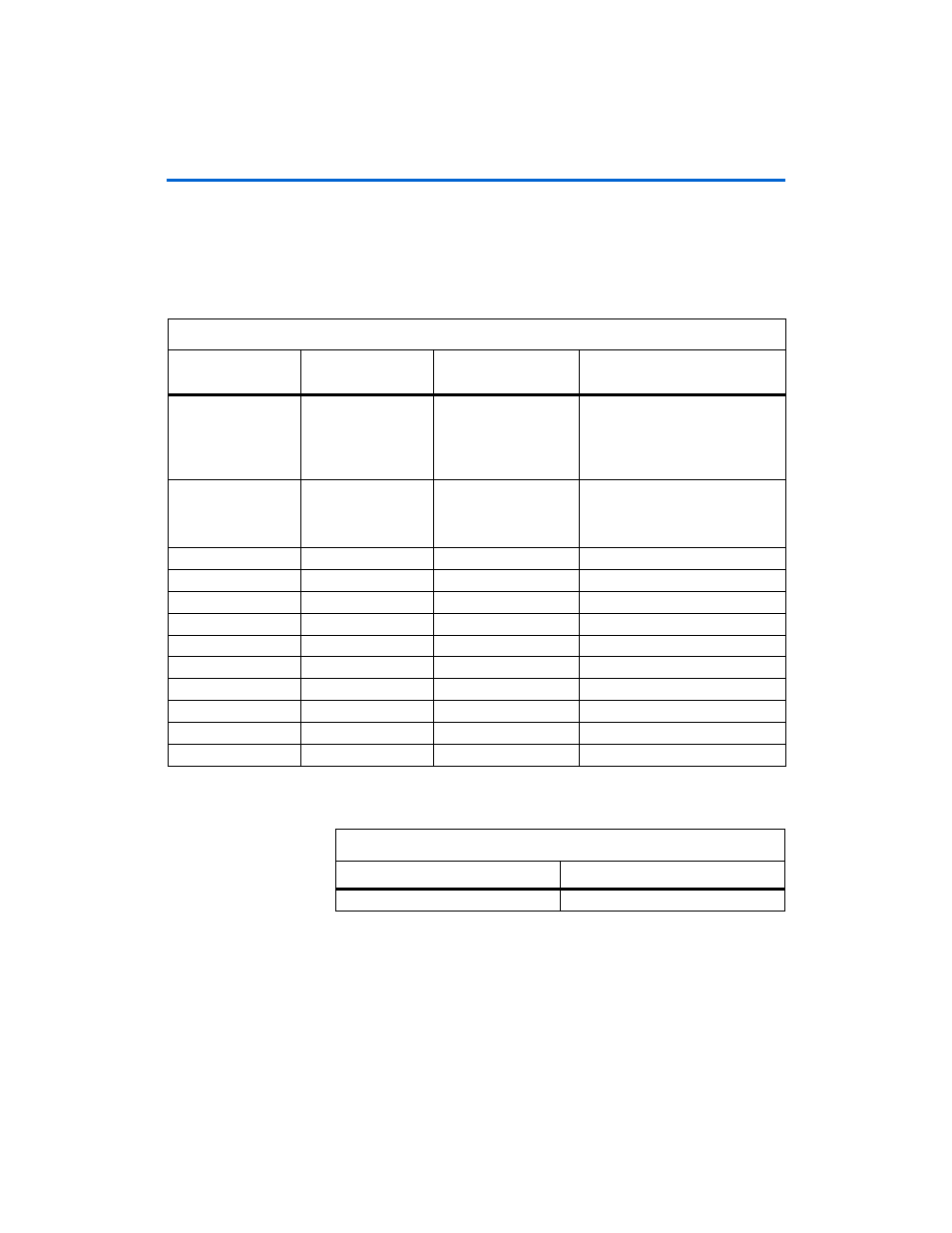
Table 2–7
lists the required signals for the flash memory. Flash signals are
routed from the Spansion flash device to the MAX II device. The required
signals are then routed from the MAX II device to the Arria GX device
(see
Figure 2–4
). Signal directions are relative to the MAX II device as far
as direction and signaling standard.
Table 2–8
shows configuration file sizes for the Arria GX device.
Table 2–7. Flash Interface I/O
MAX II Pin Numbers
Schematic
Signal Name
Description
Signal Type
K2,K3,H4,J4,K4,
J5,K5,K6, J6,K7,
K8,H7,J8,H8,K10,
J9,H9,J10,H10,G8
G9,G10,F10,F9
FLASH_A(24:0)
Address bus
3.3-V CMOS out (25 bit)
C2,B1,C1,D3,D2,
D1,E3,F2,F3,F1,
G1,H1,G2,G3,K1,
J3
FLASH_D(15:0)
Data bus
3.3-V CMOS in/out (16 bit)
F2
FLASH_CEn
Chip enable
3.3-V CMOS out
B5
FLASH_RESETn
Reset
N/A (Tie to VCC)
G2
FLASH_OEn
Output enable
3.3-V CMOS out
A5
FLASH_WEn
Write enable
3.3-V CMOS out
B4
FLASH_WPn
Write protect
N/A (Tie to VCC)
A4
FLASH_RDYBSYn
Ready/not busy
No connect (Tie to VCC)
F7
FLASH_BYTEn
Byte/word select
N/A (Tie to VCC)
VIO
I/O power
3.3-V
VCC
Core power
3.3-V
VSS
Ground
Ground
Table 2–8. Configuration File Sizes
Device
Configuration File Size (Mb)
EP1AGX60DF780C6N
16,951,824