Configuration push button (s5), Configuration push button (s5) -14 – Altera Arria GX Development Board User Manual
Page 24
2–14
Reference Manual
Altera Corporation
Arria GX Development Board
October 2007
Configuration Schemes
Configuration Push Button (S5)
Board reference S5 is a push-button with a direct connection to the
Arria GX device’s CONFIGn signal that—upon pressing to drive low—
forces a reconfiguration of the FPGA from the on board flash memory.
The Arria GX device’s pin name associated with the CONFIGn signal is
V16
.
1
Pushing the S5 switch causes the FPGA to reload a configuration
from the on-board flash device.
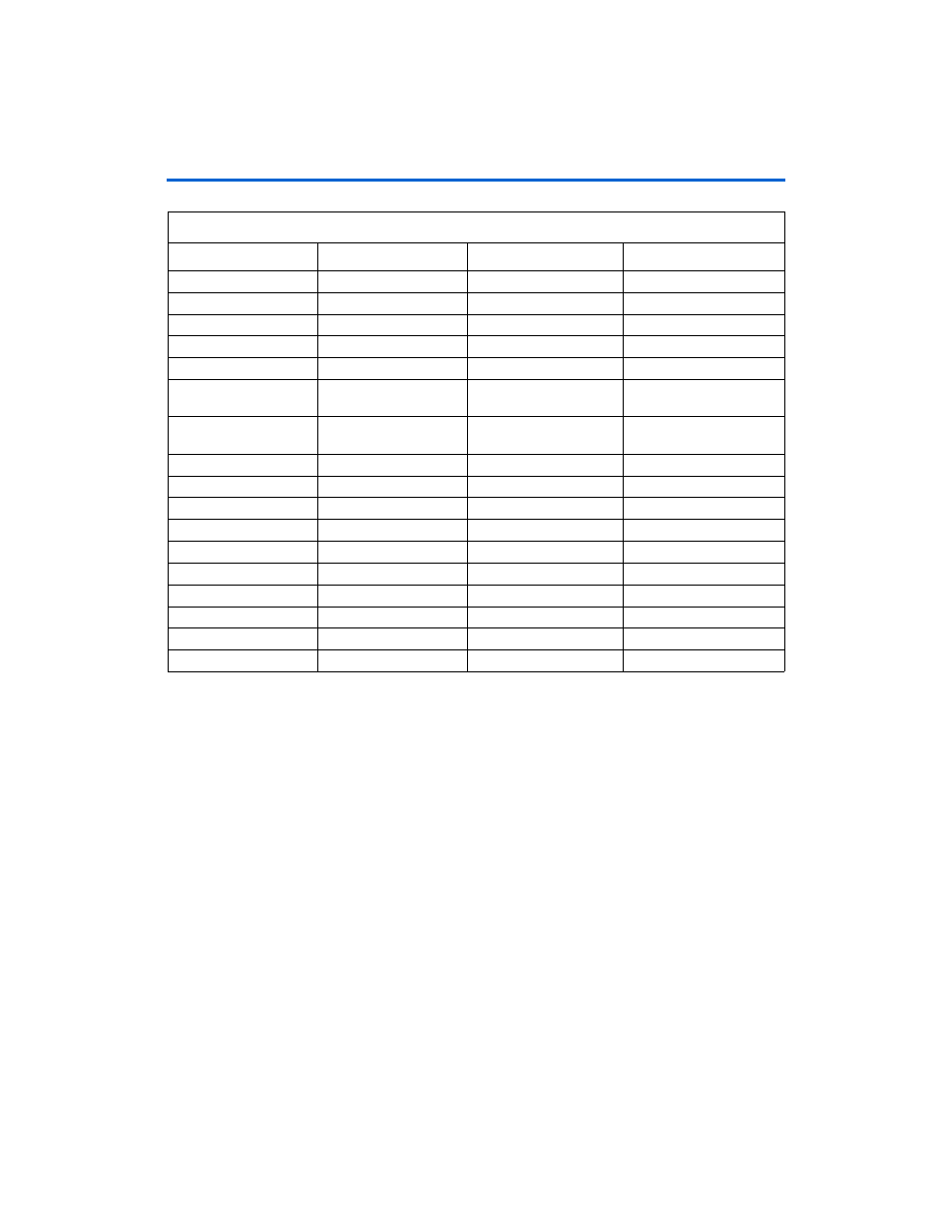
G2
FLASH_OEn
Flash output enable
3.3-V CMOS out
A5
FLASH_WEn
Flash write enable
3.3-V CMOS out
A1,B2
CONFIG_MODE(1:0)
Configuration mode input
3.3-V CMOS in
A3,A2,B3,C3
MSEL(3:0)
FPGA mode select output
3.3-V CMOS out
E2
MAX_EN
Enables operation for PFL
3.3-V CMOS in
A9,B6,A8
FPGA_PGM(2:0)
Remote configuration
page select
3.3-V CMOS in
C8,B9,A10
DIPSW_PGM(2:0)
DIP switch configuration
page select
3.3-V CMOS in
E1,E2
MAXII_CLK_IN
100-MHz clock input
3.3-V CMOS in
J1
TMS
JTAG mode select
N/A
H2
TDI
JTAG data in
N/A
J2
TDO
JTAG data out
N/A
H3
TCK
JTAG clock
N/A
VCCIO1
I/O bank 1 power
3.3 V
VCCIO2
I/O bank 2 power
3.3 V
VCCINT
Core power
3.3 V
GNDIO
I/O GND
GND
GNDINT
Core GND
GND
Table 2–10. MAX II CPLD Signals & I/O Requirements (Part 2 of 2)
MAX II Pin Numbers
Schematic Signal Name
Description
Signal Type