Flash memory (u5), Flash memory (u5) –11 – Altera Nios Development Board Stratix II Edition User Manual
Page 21
Altera Corporation
Reference Manual
2–11
May 2007
Nios Development Board Stratix II Edition
Board Components
Flash Memory
(U5)
U5 is an 8-bit, 16 MByte AMD flash memory device connected to the
FPGA. The part number is S29GL128M10TFIR1. Refer to
for
connections between the FPGA and the flash memory chip. U5 can be
used for two purposes:
1.
A Nios II embedded processor implemented on the FPGA can use
the flash memory as general-purpose memory and non-volatile
storage.
2.
The flash memory can hold FPGA configuration data that is used by
the configuration controller to load the FPGA at power-up. Refer to
“Configuration Controller Device (U3)” on page 2–33
for related
information.
A Nios II processor design in the FPGA can identify the 16 MByte flash
memory in its address space, and can program new data (either new
FPGA configuration data, Nios II software, or both) into flash memory.
The Nios II development software includes subroutines for writing and
erasing flash memory.
1
The flash memory device shares address and data connections
with the Ethernet MAC/PHY device.
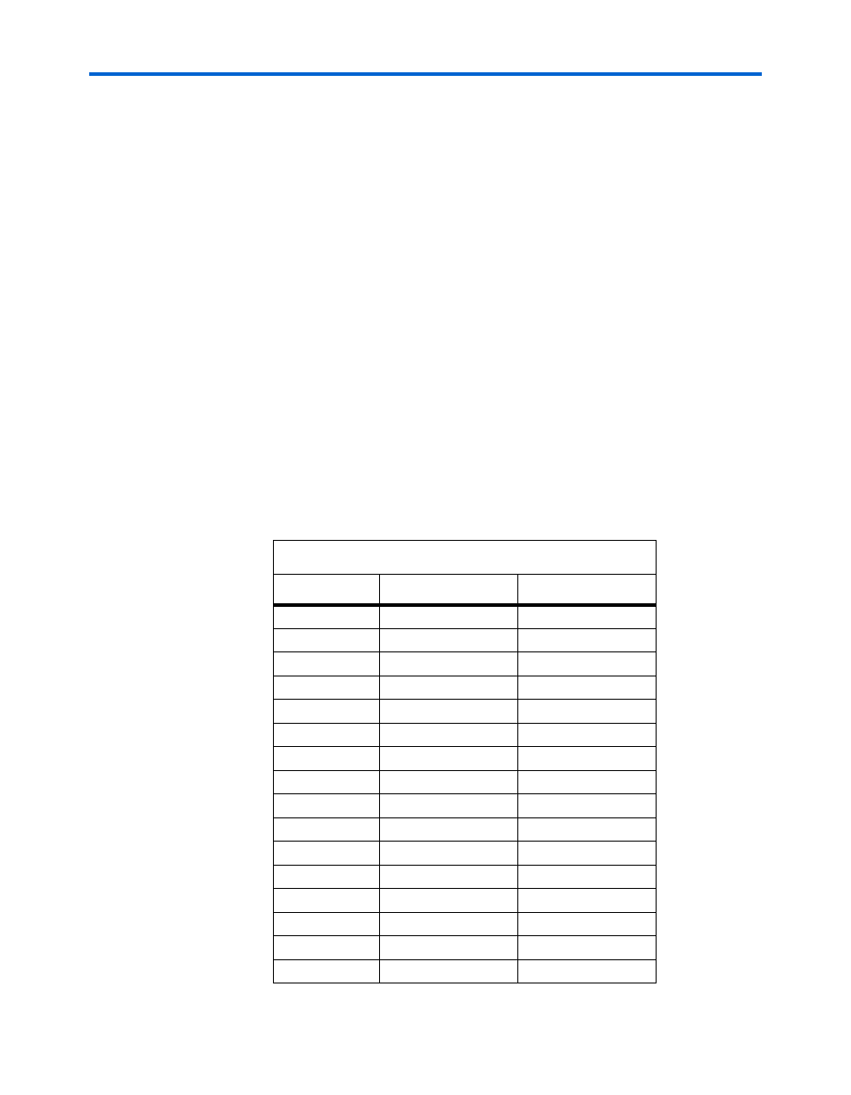
Table 2–8. Flash Memory Pin Table
FPGA Pin
U5 Pin
Board Net Name
V25
51
fe_a0
U26
31
fe_a1
U25
26
fe_a2
T25
25
fe_a3
T24
24
fe_a4
V20
23
fe_a5
V19
22
fe_a6
U20
21
fe_a7
U19
20
fe_a8
T22
10
fe_a9
T21
9
fe_a10
T20
8
fe_a11
T19
7
fe_a12
U22
6
fe_a13
U21
5
fe_a14
V22
4
fe_a15