Figure 2–21, Fpga (u62) plls, Clock buffer (u2) – Altera Nios Development Board Stratix II Edition User Manual
Page 52
Advertising
2–42
Reference Manual
Altera Corporation
Nios Development Board Stratix II Edition
May 2007
Board Components
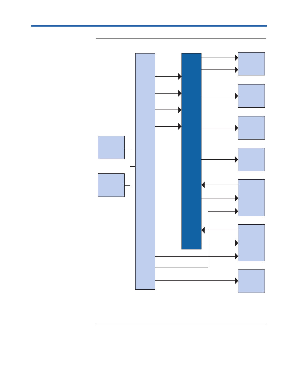
Figure 2–21. Clock Circuitry
Note to
:
(1)
To use an external clock signal, remove the crystal oscillator from its socket. Make
sure to note the correct orientation of the oscillator before removing it.
osc_CLK0
osc_CLK1
sram_CLKIN
sdram_CLKIN
MAX (U3)
cpld_CLKOSC
osc_CLK3
osc_CLK2 DDR SDRAM (U63)
SSRAM (U74)
sram_CLK
PMC_CLK
PMC (JH1 & JH2)
FPGA
(U62)
PLLs
PROTO1
proto1_PLLCLK
proto1_CLKOUT
proto1_OSCCLK
Mictor (J25)
mictor_CLK
PROTO2
proto2_PLLCLK
proto2_CLKOUT
proto2_OSCCLK
SMA External
Input (J4)
Oscillator (Y2)
Clock
Buffer
(U2)
Advertising