Power-supply circuitry, Power-supply circuitry –44, R to – Altera Nios Development Board Stratix II Edition User Manual
Page 54
2–44
Reference Manual
Altera Corporation
Nios Development Board Stratix II Edition
May 2007
Board Components
Power-Supply
Circuitry
The Nios development board runs on a 16.0 V, unregulated, input power
supply connected to J26. On-board circuitry generates ±12.0 V, +5.0 V,
+3.3 V, +2.5 V, and +1.2 V regulated power levels. For applications
requiring high current, separate voltage levels can be supplied from a
workbench power supply.
■
The input power-supply on J26 can be either center-negative or
center-positive. A bridge rectifier (D34) presents the appropriate
polarity to the voltage regulators.
■
The 5.0 V supply is presented on pin 2 of J12 and J15 for use by any
device plugged into the PROTO1 & PROTO2 expansion connectors.
■
The 3.3 V supply is used as the power source for all FPGA I/O pins.
The 3.3 V supply is also available for PROTO1 & PROTO2 daughter
cards.
■
The 2.5 V supply is used only as the power supply for the DDR
SDRAM chip and is not available on any connector or header.
■
The 1.2 V supply is used only as the power supply for the Stratix II
device core (VCCINT) and it is not available on any connector or
header.
■
The ±12.0 V supply is provided for the PMC connectors JH1 and JH2.
Refer to
“PMC Connector (JH1 & JH2)” on page 2–26
for more
details. When workbench power supplies are connected to the board,
a corresponding fuse must be removed to decouple the on-board
voltage regulator. Each on-board regulator drives power through a
7 A fuse. Refer to
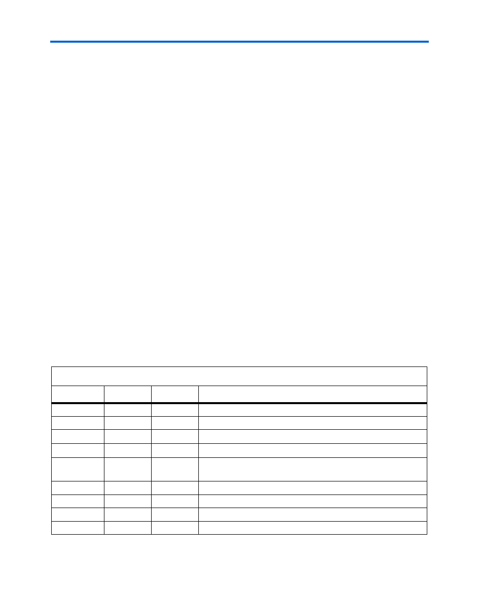
.
lists the details of what voltage levels can be supplied to what
points on the board.
Table 2–23. Power Supply and Fuse Details
Voltage
Pad
Fuse
Note
1.2V
J30
F3
Core power for FPGA.
1.2V
TP12
F7
FPGA PLL power supply.
1.25V
TP10
F5
DDR SDRAM I/O V
TT
.
1.25V
TP9
F4
DDR SDRAM I/O V
REF
.
2.5V
TP11
F6
DDR SDRAM VDD power supply. FPGA V
CCIO
for pins that
interface to DDR SDRAM.
3.3V
J29
F2
3.3 V power for multiple components on the board.
5V
J28
F1
5.0 V power for multiple components on the board.
+12V
J31
F8
Power for the PMC connectors.
-12V
TP13
F9
Power for the PMC connectors.