Altera Nios Development Board Stratix II Edition User Manual
Page 27
Altera Corporation
Reference Manual
2–17
May 2007
Nios Development Board Stratix II Edition
Board Components
■
41 I/O pins for prototyping. All 41 I/O pins connect to user I/O pins
on the FPGA. Each signal passes through analog switches to protect
the FPGA from 5.0 V logic levels. These analog switches are
permanently enabled. The output logic-level on the expansion
prototype connector pins is 3.3 V.
●
PROTO1 switches: U19, U20, U21, U22 and U25
●
PROTO2 switches: U27, U28, U29, U30 and U31
■
A buffered, zero-skew copy of the on-board oscillator output from
U2.
■
A buffered, zero-skew copy of the FPGA phase-locked loop (PLL)
output.
■
A power-on reset signal that is asserted low.
■
Five regulated 3.3 V power-supply pins (2 A total max load for both
PROTO1 & PROTO2).
■
One regulated 5.0 V power-supply pin (1 A total max load for both
PROTO1 & PROTO2).
■
Numerous ground connections.
The PROTO1 expansion prototype connector shares FPGA I/O pins with
the CompactFlash connector (CON3). Designs can use either the PROTO1
connector or the CompactFlash connector.
1
Do not connect cards to PROTO1 and CON3 at the same time.
Damage to one or both cards might result.
f
See the Altera web site for a list of available expansion daughter cards
that can be used with the Nios development board at
www.altera.com/devkits.
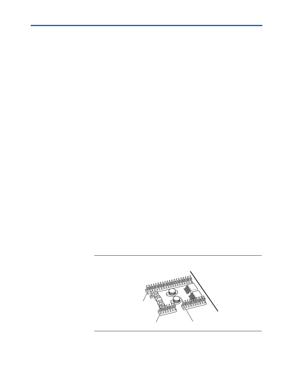
show connections from the
PROTO1 expansion headers to the FPGA.
Figure 2–6. PROTO1 Expansion Prototype Connector - J11, J12 & J13
Pin 1
J11
J12
J13
Pin 1
Pin 1